
Page 32 - MEMS Mechanical Sensors
P. 32
2.3 Fabrication Techniques 21
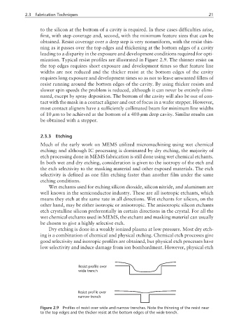
to the silicon at the bottom of a cavity is required. In these cases difficulties arise,
first, with step coverage and, second, with the minimum feature sizes that can be
obtained. Resist coverage over a deep step is very nonuniform, with the resist thin-
ning as it passes over the top edges and thickening at the bottom edges of a cavity
leading to a disparity in the exposure and development conditions required for opti-
mization. Typical resist profiles are illustrated in Figure 2.9. The thinner resist on
the top edges requires short exposure and development times so that feature line
widths are not reduced and the thicker resist at the bottom edges of the cavity
requires long exposure and development times so as not to leave unwanted fillets of
resist running around the bottom edges of the cavity. By using thicker resists and
slower spin speeds the problem is reduced, although it can never be entirely elimi-
nated, except by spray deposition. The bottom of the cavity will also be out of con-
tact with the mask in a contact aligner and out of focus in a wafer stepper. However,
most contact aligners have a sufficiently collimated beam for minimum line widths
of 10 µm to be achieved at the bottom of a 400-µm deep cavity. Similar results can
be obtained with a stepper.
2.3.3 Etching
Much of the early work on MEMS utilized micromachining using wet chemical
etching; and although IC processing is dominated by dry etching, the majority of
etch processing done in MEMS fabrication is still done using wet chemical etchants.
In both wet and dry etching, consideration is given to the isotropy of the etch and
the etch selectivity to the masking material and other exposed materials. The etch
selectivity is defined as one film etching faster than another film under the same
etching conditions.
Wet etchants used for etching silicon dioxide, silicon nitride, and aluminum are
well known in the semiconductor industry. These are all isotropic etchants, which
means they etch at the same rate in all directions. Wet etchants for silicon, on the
other hand, may be either isotropic or anisotropic. The anisotropic silicon etchants
etch crystalline silicon preferentially in certain directions in the crystal. For all the
wet chemical etchants used in MEMS, the etchant and masking material can usually
be chosen to give a highly selective etch.
Dry etching is done in a weakly ionized plasma at low pressure. Most dry etch-
ing is a combination of chemical and physical etching. Chemical etch processes give
good selectivity and isotropic profiles are obtained, but physical etch processes have
low selectivity and induce damage from ion bombardment. However, physical etch
Resist profile over
wide trench
Resist profile over
narrow trench
Figure 2.9 Profiles of resist over wide and narrow trenches. Note the thinning of the resist near
to the top edges and the thicker resist at the bottom edges of the wide trench.