Page 141 - MEMS and Microstructures in Aerospace Applications
P. 141
Osiander / MEMS and microstructures in Aerospace applications  DK3181_c007 Final Proof page 130 1.9.2005 12:03pm


                   130                       MEMS and Microstructures in Aerospace Applications


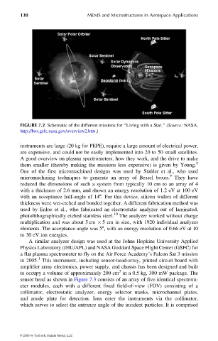
                   FIGURE 7.2 Schematic of the different missions for ‘‘Living with a Star.’’ (Source: NASA,
                   http://lws.gsfc.nasa.gov/overview2.htm.)

                   instruments are large (20 kg for PEPE), require a large amount of electrical power,
                   are expensive, and could not be easily implemented into 20 to 50 small satellites.
                   A good overview on plasma spectrometers, how they work, and the drive to make
                   them smaller (thereby making the missions less expensive) is given by Young. 8
                   One of the first micromachined designs was used by Stalder et al., who used
                                                                            9
                   micromachining techniques to generate an array of Bessel boxes. They have
                   reduced the dimensions of such a system from typically 10 cm to an array of 4
                   with a thickness of 2.6 mm, and shown an energy resolution of 1.2 eV at 100 eV
                   with an acceptance half-angle of 148. For this device, silicon wafers of different
                   thickness were wet-etched and bonded together. A different fabrication method was
                   used by Enloe et al., who fabricated an electrostatic analyzer out of laminated,
                   photolithographically etched stainless steel. 10  The analyzer worked without charge
                   multiplication and was about 5 cm   5 cm in size, with 1920 individual analyzer
                   elements. The acceptance angle was 58, with an energy resolution of 0.66 eV at 10
                   to 30 eV ion energies.
                       A similar analyzer design was used at the Johns Hopkins University Applied
                   Physics Laboratory (JHU/APL) and NASA Goddard Space Flight Center (GSFC) for
                   a flat plasma spectrometer to fly on the Air Force Academy’s Falcon Sat 3 mission
                          1
                   in 2005. This instrument, including sensor-head-array, printed circuit board with
                   amplifier array electronics, power supply, and chassis has been designed and built
                                                         3
                   to occupy a volume of approximately 200 cm in a 0.5 kg, 300 mW package. The
                   sensor head as shown in Figure 7.3 consists of an array of five identical spectrom-
                   eter modules, each with a different fixed field-of-view (FOV) consisting of a
                   collimator, electrostatic analyzer, energy selector masks, microchannel plates,
                   and anode plate for detection. Ions enter the instruments via the collimator,
                   which serves to select the entrance angle of the incident particles. It is comprised


                   © 2006 by Taylor & Francis Group, LLC

