
Page 142 - MEMS and Microstructures in Aerospace Applications
P. 142
Osiander / MEMS and microstructures in Aerospace applications DK3181_c007 Final Proof page 131 1.9.2005 12:03pm
Microtechnologies for Science Instrumentation Applications 131
15 mm
collimator
aperture
top energy
selector mask collimator
bottom energy electrostatic 8 mm
selector mask analyzer
MCP
anode
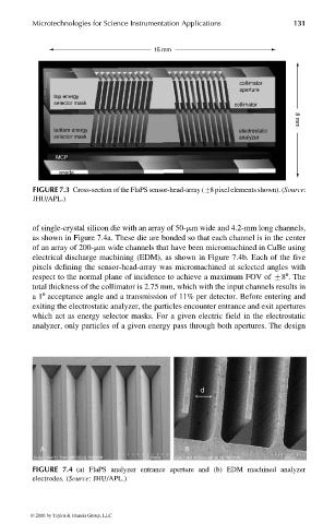
FIGURE 7.3 Cross-section of the FlaPS sensor-head-array (+8 pixel elements shown). (Source:
JHU/APL.)
of single-crystal silicon die with an array of 50-mm wide and 4.2-mm long channels,
as shown in Figure 7.4a. These die are bonded so that each channel is in the center
of an array of 200-mm wide channels that have been micromachined in CuBe using
electrical discharge machining (EDM), as shown in Figure 7.4b. Each of the five
pixels defining the sensor-head-array was micromachined at selected angles with
respect to the normal plane of incidence to achieve a maximum FOV of +88.The
total thickness of the collimator is 2.75 mm, which with the input channels results in
a18 acceptance angle and a transmission of 11% per detector. Before entering and
exiting the electrostatic analyzer, the particles encounter entrance and exit apertures
which act as energy selector masks. For a given electric field in the electrostatic
analyzer, only particles of a given energy pass through both apertures. The design
FIGURE 7.4 (a) FlaPS analyzer entrance aperture and (b) EDM machined analyzer
electrodes. (Source: JHU/APL.)
© 2006 by Taylor & Francis Group, LLC