
Page 317 - MEMS and Microstructures in Aerospace Applications
P. 317
Osiander / MEMS and microstructures in Aerospace applications DK3181_c014 Final Proof page 311 1.9.2005 12:47pm
Material Selection for Applications of MEMS 311
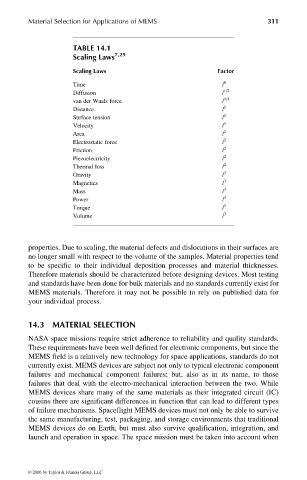
TABLE 14.1
Scaling Laws 7,29
Scaling Laws Factor
Time l 0
1/2
Diffusion l
1/4
van der Waals force l
Distance l 1
Surface tension l 1
Velocity l 1
Area l 2
Electrostatic force l 2
Friction l 2
Piezoelectricity l 2
Thermal loss l 2
Gravity l 3
Magnetics l 3
Mass l 3
Power l 3
Torque l 3
Volume l 3
properties. Due to scaling, the material defects and dislocations in their surfaces are
no longer small with respect to the volume of the samples. Material properties tend
to be specific to their individual deposition processes and material thicknesses.
Therefore materials should be characterized before designing devices. Most testing
and standards have been done for bulk materials and no standards currently exist for
MEMS materials. Therefore it may not be possible to rely on published data for
your individual process.
14.3 MATERIAL SELECTION
NASA space missions require strict adherence to reliability and quality standards.
These requirements have been well defined for electronic components, but since the
MEMS field is a relatively new technology for space applications, standards do not
currently exist. MEMS devices are subject not only to typical electronic component
failures and mechanical component failures; but, also as in its name, to those
failures that deal with the electro-mechanical interaction between the two. While
MEMS devices share many of the same materials as their integrated circuit (IC)
cousins there are significant differences in function that can lead to different types
of failure mechanisms. Spaceflight MEMS devices must not only be able to survive
the same manufacturing, test, packaging, and storage environments that traditional
MEMS devices do on Earth, but must also survive qualification, integration, and
launch and operation in space. The space mission must be taken into account when
© 2006 by Taylor & Francis Group, LLC