
Page 46 - MEMS and Microstructures in Aerospace Applications
P. 46
Osiander / MEMS and microstructures in Aerospace applications DK3181_c003 Final Proof page 37 1.9.2005 8:59pm
MEMS Fabrication 37
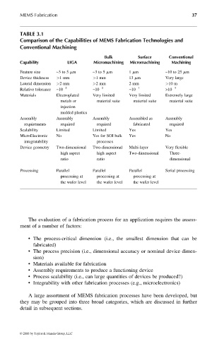
TABLE 3.1
Comparison of the Capabilities of MEMS Fabrication Technologies and
Conventional Machining
Bulk Surface Conventional
Capability LIGA Micromachining Micromachining Machining
Feature size ~3 to 5 mm ~3 to 5 mm 1 mm ~10 to 25 mm
Device thickness >1mm >1mm 13 mm Very large
Lateral dimension >2mm >2mm 2mm >10 m
2 2 1 3
Relative tolerance ~10 ~10 ~10 >10
Materials Electroplated Very limited Very limited Extremely large
metals or material suite material suite material suite
injection
molded plastics
Assembly Assembly Assembly Assembled as Assembly
requirements required required fabricated required
Scalability Limited Limited Yes Yes
MicroElectronic No Yes for SOI bulk Yes No
integratability processes
Device geometry Two-dimensional Two-dimensional Multi-layer Very flexible
high aspect high aspect Two-dimensional Three-
ratio ratio dimensional
Processing Parallel Parallel Parallel Serial processing
processing at processing at processing at
the wafer level the wafer level the wafer level
The evaluation of a fabrication process for an application requires the assess-
ment of a number of factors:
. The process-critical dimension (i.e., the smallest dimension that can be
fabricated)
. The process precision (i.e., dimensional accuracy or nominal device dimen-
sion)
. Materials available for fabrication
. Assembly requirements to produce a functioning device
. Process scalability (i.e., can large quantities of devices be produced?)
. Integrability with other fabrication processes (e.g., microelectronics)
A large assortment of MEMS fabrication processes have been developed, but
they may be grouped into three broad categories, which are discussed in further
detail in subsequent sections.
© 2006 by Taylor & Francis Group, LLC