
Page 24 -
P. 24
Materials for Microelectromechanical Systems 2-5
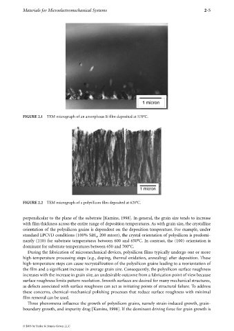
FIGURE 2.1 TEM micrograph of an amorphous Si film deposited at 570°C.
FIGURE 2.2 TEM micrograph of a polysilicon film deposited at 620°C.
perpendicular to the plane of the substrate [Kamins, 1998]. In general, the grain size tends to increase
with film thickness across the entire range of deposition temperatures. As with grain size, the crystalline
orientation of the polysilicon grains is dependent on the deposition temperature. For example, under
standard LPCVD conditions (100% SiH , 200 mtorr), the crystal orientation of polysilicon is predomi-
4
nantly (110) for substrate temperatures between 600 and 650°C. In contrast, the (100) orientation is
dominant for substrate temperatures between 650 and 700°C.
During the fabrication of micromechanical devices, polysilicon films typically undergo one or more
high-temperature processing steps (e.g., doping, thermal oxidation, annealing) after deposition. These
high-temperature steps can cause recrystallization of the polysilicon grains leading to a reorientation of
the film and a significant increase in average grain size. Consequently, the polysilicon surface roughness
increases with the increase in grain size, an undesirable outcome from a fabrication point of view because
surface roughness limits pattern resolution. Smooth surfaces are desired for many mechanical structures,
as defects associated with surface roughness can act as initiating points of structural failure. To address
these concerns, chemical–mechanical polishing processes that reduce surface roughness with minimal
film removal can be used.
Three phenomena influence the growth of polysilicon grains, namely strain-induced growth, grain-
boundary growth, and impurity drag [Kamins, 1998]. If the dominant driving force for grain growth is
© 2006 by Taylor & Francis Group, LLC