
Page 26 -
P. 26
Materials for Microelectromechanical Systems 2-7
implanted dopant, as well as to repair implant-related damage in the polysilicon film. In general, the resis-
tivity of implanted polysilicon films is not as low as films doped by diffusion. In addition, the need for
specialized implantation equipment limits the use of this method in polysilicon MEMS.
The electrical properties of polysilicon depend strongly on the grain structure of the film. The grain
boundaries provide a potential barrier to the moving charge carriers, thus affecting the conductivity of
the films. For P-doped polysilicon, the resistivity decreases as the amount of P increases for concentrations
4
3
21
up to about 1 10 /cm .Above this value, the resistivity reaches a plateau of about 4 10 Ω-cm after
2
a 1000°C anneal. The maximum mobility for such a highly P-doped polysilicon is about 30cm /Vs. Grain
boundary and ionized impurity scattering are important factors limiting the mobility [Kamins, 1988].
The thermal conductivity of polysilicon is a strong function of the grain structure of the film [Kamins
1998]. For fine-grain films, the thermal conductivity is about 0.30 to 0.35 W/cm-K, which is about 20 to
25% of the single-crystal value. For thick films with large grains, the thermal conductivity ranges between
50 and 85% of the single-crystal value.
In general, thin films are generally under a state of stress commonly referred to as residual stress, and
polysilicon is no exception. In polysilicon micromechanical structures, the residual stress in the films can
greatly affect the performance of the device. Like the electrical and thermal properties of polysilicon, the
as-deposited residual stress in polysilicon films depends on microstructure. In general, as-deposited poly-
silicon films have compressive residual stresses, although reports regarding polysilicon films with tensile
stress can be found in the literature [Kim et al., 1998]. The highest compressive stresses are found in
amorphous Si films and polysilicon films with a strong columnar (110) texture. For films with fine-
grained microstructures, the stress tends to be tensile. For the same deposition conditions, thick polysil-
icon films tend to have lower residual stress values than thin films; this is especially true for films with a
columnar microstructure. Annealing can be used to reduce the compressive stress in as-deposited poly-
silicon films. For polysilicon films doped with phosphorus by diffusion, a decrease in the magnitude of
compressive stress has been correlated with grain growth [Kamins, 1998]. For polysilicon films deposited
9
2
9
at 650°C, the compressive residual stress is typically on the order of 5 10 to 10 10 dyne/cm .
8
2
However, these stresses can be reduced to less than 10 dyne/cm by annealing the films at high temper-
ature (1000°C) in a N ambient [Guckel et al., 1985; Howe and Muller, 1983]. Compressive stresses in
2
10
fine-grained polysilicon films deposited at 580°C (100-Å grain size) can be reduced from 1.5 10 to
2
2
8
9
less than 10 dyne/cm by annealing above 1000°C, or even can be made to be tensile (5 10 dynes/cm )
by annealing at temperatures between 650 and 850°C [Guckel et al., 1988]. Advances in the area of rapid
thermal annealing (RTA) as applied to polysilicon indicate that RTA is a fast and effective method of stress
reduction in polysilicon films. For polysilicon films deposited at 620°C with compressive stresses of about
340MPa, a 10 sec anneal at 1100°C was sufficient to completely relieve the stress [Zhang et al., 1998].
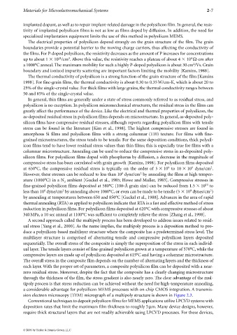
A second approach called the multipoly process has been developed to address issues related to resid-
ual stress [Yang et al., 2000]. As the name implies, the multipoly process is a deposition method to pro-
duce a polysilicon-based multilayer structure where the composite has a predetermined stress level. The
multilayer structure is comprised of alternating tensile and compressive polysilicon layers deposited
sequentially. The overall stress of the composite is simply the superposition of the stress in each individ-
ual layer. The tensile layers consist of fine-grained polysilicon grown at a temperature of 570°C, while the
compressive layers are made up of polysilicon deposited at 615°C and having a columnar microstructure.
The overall stress in the composite film depends on the number of alternating layers and the thickness of
each layer. With the proper set of parameters, acomposite polysilicon film can be deposited with a near-
zero residual stress. Moreover, despite the fact that the composite has a clearly changing microstructure
through the thickness of the film, the stress gradient is also nearly zero. The clear advantage of the mul-
tipoly process is that stress reduction can be achieved without the need for high-temperature annealing,
aconsiderable advantage for polysilicon MEMS processes with on-chip CMOS integration. Atransmis-
sion electron microscopy (TEM) micrograph of amultipoly structure is shown in Figure 2.3.
Conventional techniques to deposit polysilicon films for MEMS applications utilize LPCVD systems with
deposition rates that limit the maximum film thickness to roughly 5µm. Many device designs, however,
require thick structural layers that are not readily achievable using LPCVD processes. For these devices,
© 2006 by Taylor & Francis Group, LLC