
Page 27 -
P. 27
2-8 MEMS: Design and Fabrication
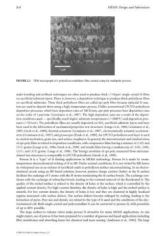
FIGURE 2.3 TEM micrograph of a polysilicon multilayer film created using the multipoly process.
wafer bonding and etchback techniques are often used to produce thick ( 10µm) single-crystal Si films
on sacrificial substrate layers. There is, however, a deposition technique to produce thick polysilicon films
on sacrificial substrates. These thick polysilicon films are called epi-poly films because epitaxial Si reac-
tors are used to deposit them using a high-temperature process. Unlike conventional LPCVD polysilicon
deposition processes, which have deposition rates of 100Å/min, epi-poly processes have deposition rates
on the order of 1 µm/min [Gennissen et al., 1997]. The high deposition rates are a result of the deposi-
tion conditions used — specifically, much higher substrate temperatures ( 1000°C) and deposition pres-
sures ( 50 torr). The polysilicon films are usually deposited on SiO sacrificial substrate layers and have
2
been used in the fabrication of mechanical properties test structures [Lange et al., 1996; Gennissen et al.,
1997; Greek et al., 1999], thermal actuators [Gennissen et al., 1997], electrostatically actuated accelerom-
eters [Gennissen et al., 1997], and gryoscopes [Funk et al., 1999]. An LPCVD polysilicon seed layer is used
to control nucleation, grain size, and surface roughness. In general, the microstructure and residual stress
of epi-poly films is related to deposition conditions, with compressive films having a mixture of (110) and
(311) grains [Lange et al., 1996; Greek et al., 1999] and tensile films having a random mix of (110), (100),
(111), and (311) grains [Lange et al., 1996]. The Young’s modulus of epi-poly measured from microma-
chined test structures is comparable to LPCVD polysilicon [Greek et al., 1999].
Porous Si is a “type” of Si finding applications in MEMS technology. Porous Si is made by room-
temperature electrochemical etching of Si in HF. Under normal conditions, Si is not etched by HF, hence
its widespread use as an etchant of sacrificial oxide in polysilicon surface micromachining. In an electro-
chemical circuit using an HF-based solution, however, positive charge carriers (holes) at the Si surface
facilitate the exchange of F atoms with the H atoms terminating the Si surface bonds. The exchange con-
tinues with the exchange of subsurface bonds, leading to the eventual removal of the fluorinated Si. The
quality of the etched surface is related to the density of holes at the surface, which is controlled by the
applied current density. For high current densities, the density of holes is high and the etched surface is
smooth. For low current density, the density of holes is low and they are clustered in highly localized
regions associated with surface defects. The surface defects become enlarged by etching, leading to the
formation of pores. Pore size and density are related to the type of Si used and the conditions of the elec-
trochemical cell. Both single-crystal and polycrystalline Si can be converted to porous Si, with porosities
of up to 80% possible.
The large surface-to-volume ratios make porous Si attractive for many MEMS applications. As one
might expect, use of porous Si has been proposed for a number of gaseous and liquid applications including
filter membranes and absorbing layers for chemical and mass sensing [Anderson et al., 1994]. The large
© 2006 by Taylor & Francis Group, LLC