
Page 38 -
P. 38
Materials for Microelectromechanical Systems 2-19
SF combined with O and sometimes with an inert gas or H are used. The high oxygen content in these
6 2 2
plasmas generally prohibits the use of photoresist as a masking material; therefore, hard masks made of
metals such as Al and Ni are often used. RIE processes are generally effective patterning techniques; how-
ever, a phenomenon called micromasking, which results in the formation of etch-field grass, can some-
times be a problem. Nonetheless, RIE-based SiC surface-micromachining processes using polysilicon and
SiO sacrificial layers have been developed [Fleischman et al., 1996, 1998]. These processes are effective
2
means to fabricate single-layer SiC structures, but multilayer structures are very difficult to fabricate
because the etch rates of the sacrificial layers are much higher than the SiC structural layers. The lack of
arobust etch stop makes critical dimensional control in the thickness direction unreliable, thus making
RIE-based SiC multilayer processes impractical.
To address the materials compatibility issues facing RIE-based SiC surface micromachining in the
development of amultilayer process, a micromolding process for SiC patterning on sacrificial layer sub-
strates has been developed [Yasseen et al., 2000]. In essence, the micromolding technique is the thin film
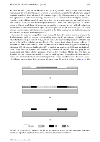
analog to the molding technique presented earlier. The cross-sectional schematic shown in Figure 2.6
illustrates the steps to fabricate a SiC lateral resonant structure. The micromolding process utilizes poly-
silicon and SiO films as sacrificial molds, Si N as an electrical insulator, and SiO as a sacrificial sub-
2 3 4 2
strate. These films are deposited and patterned by conventional methods, thus leveraging the well
characterized and highly selective processes developed for polysilicon MEMS. Poly-SiC films are
deposited into and onto the micromolds. Mechanical polishing with a diamond-based slurry is used to
remove poly-SiC from atop the molds, then the appropriate etchant is used to dissolve the molds and sac-
rificial layers. An example of device structure fabricated using this method is shown in Figure 2.7. The
(a)
(b)
(c)
Oxide Si SiC Poly
FIGURE 2.6 Cross-sectional schematics of the SiC micromolding process: (a) after micromold fabrication,
(b) after SiC deposition and planarization, and (c) after mold and sacrificial layer release.
© 2006 by Taylor & Francis Group, LLC