
Page 39 -
P. 39
2-20 MEMS: Design and Fabrication
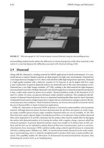
FIGURE 2.7 SEM micrograph of a SIC lateral resonant structure fabricated using the micromolding process.
micromolding method clearly utilizes the differences in chemical properties of the three materials in this
system in a way that bypasses the difficulties associated with chemical etching of SiC.
2.9 Diamond
Along with SiC, diamond is a leading material for MEMS applications in harsh environments. It is com-
monly known as nature’s hardest material, an ideal property for high-wear environments. Diamond has
a very large electronic bandgap (5.5 eV) that is well suited for stable high-temperature operation. Diamond
is a high-quality insulator with a dielectric constant of 5.5; however, it can be doped with B to create
p-type conductivity. In general, diamond surfaces are chemically inert in the same environments as SiC.
35
Diamond has a very high Young’s modulus (10 GPa), making it the ideal material for high-frequency
micromachined resonators. Perhaps diamond’s only disadvantage from a materials properties perspective
is that a stable oxide cannot be grown on its surface. Thermal oxidation results in the formation of CO
and CO , which, of course, are gaseous substances under standard conditions. This complicates the fab-
2
rication of diamond-based electronic devices as deposited insulating thin films must be used. Operation
of diamond-based sensors at high temperatures requires the use of passivation coatings to protect the dia-
mond structures from oxidation. These limitations, however, can be overcome and do not severely restrict
the use of diamond films in harsh environment applications.
Unlike SiC, fabrication of diamond MEMS structures is restricted to polycrystalline and amorphous
material. Although diamond epitaxy has been demonstrated, the epi films were grown on small, irregu-
lar, single-crystalline pieces because single-crystalline diamond wafers are not yet available. 3C-SiC thin
films have been used to deposit highly oriented diamond films on Si substrates. Polycrystalline diamond
films can be deposited on Si and SiO substrates, but the surfaces often must be seeded either by damaging
2
the surface with diamond powders or by biasing the surface with a negative charge, a process called bias
enhanced nucleation. In general, diamond nucleates much more readily on Si surfaces than on SiO sur-
2
faces, and this fact can be exploited to pattern diamond films into microstructures, such as a microma-
chined atomic force microscope (AFM) cantilever probe, using a selective growth process in conjunction
with SiO molding masks [Shibata et al., 2000]. As mentioned previously, diamond can be made insulat-
2
ing or semiconducting, and it is relatively straightforward to produce both types in polycrystalline dia-
mond. This capability enables the fabrication of all-diamond microelectromechanical structures, thus
eliminating the need for Si N as an insulating layer.
3
4
© 2006 by Taylor & Francis Group, LLC