
Page 16 - Make Your Own PCBs with EAGLE from Schematic Designs to Finished Boards
P. 16
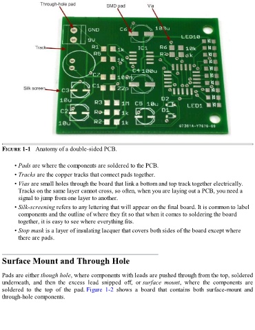
FIGURE 1-1   Anatomy of a double-sided PCB.


        • Pads are where the components are soldered to the PCB.

        • Tracks are the copper tracks that connect pads together.
        • Vias are small holes through the board that link a bottom and top track together electrically.
          Tracks on the same layer cannot cross, so often, when you are laying out a PCB, you need a

          signal to jump from one layer to another.
        • Silk-screening refers to any lettering that will appear on the final board. It is common to label

          components and the outline of where they fit so that when it comes to soldering the board
          together, it is easy to see where everything fits.
        • Stop mask is a layer of insulating lacquer that covers both sides of the board except where

          there are pads.


  Surface Mount and Through Hole


  Pads are either though hole, where components with leads are pushed through from the top, soldered
  underneath,  and  then  the  excess  lead  snipped  off,  or surface  mount,  where  the  components  are
  soldered  to  the  top  of  the  pad. Figure  1-2  shows  a  board  that  contains  both  surface-mount  and
  through-hole components.