
Page 166 - Make Your Own PCBs with EAGLE from Schematic Designs to Finished Boards
P. 166
precautions specified on the equipment and chemicals that you use.
Photoetching uses a transparency with an image of the PCB to be created printed onto
transparency film that is then placed over copper-clad board that has been presensitized. These
boards are not much more expensive than plain boards. The board is then exposed to UV light through
the transparency film.
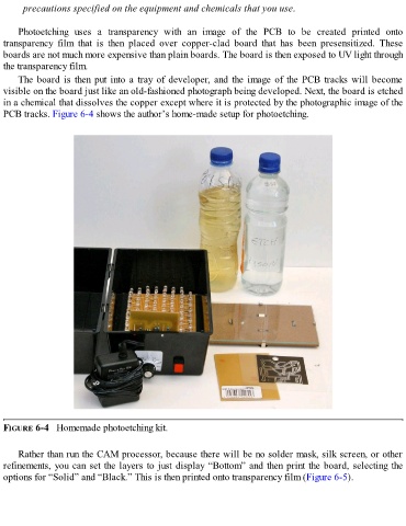
The board is then put into a tray of developer, and the image of the PCB tracks will become
visible on the board just like an old-fashioned photograph being developed. Next, the board is etched
in a chemical that dissolves the copper except where it is protected by the photographic image of the
PCB tracks. Figure 6-4 shows the author’s home-made setup for photoetching.
FIGURE 6-4 Homemade photoetching kit.
Rather than run the CAM processor, because there will be no solder mask, silk screen, or other
refinements, you can set the layers to just display “Bottom” and then print the board, selecting the
options for “Solid” and “Black.” This is then printed onto transparency film (Figure 6-5).