
Page 167 - Make Your Own PCBs with EAGLE from Schematic Designs to Finished Boards
P. 167
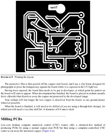
FIGURE 6-5   Printing the layout.


      The protective film is then peeled off the copper-clad board, and I use a clip frame designed for
  photographs to press the transparency against the board while it is exposed in the UV light box.

      Having been exposed, the board then needs to be put in developer, at which point the pattern on
  the board will start to appear. When development has finished, the board is placed in etchant (usually
  ferric chloride) that dissolves away the copper not protected by the developed image.

      Your etchant will last longer the less copper is dissolved from the board, so use ground planes
  wherever possible.
      When the board is finished, it will need to be drilled (if you are using a through-hole design), for
  which you will need a very fine drill bit. A diameter of 0.8 mm is ideal.


  Milling PCBs


  Low-cost  desktop  computer  numerical  control  (CNC)  routers  offer  a  chemical-free  method  of
  producing  PCBs  by  using  a  normal  copper-clad  PCB  but  then  using  a  computer-controlled  CNC
  router to cut away the unwanted copper (Figure 6-6).