
Page 155 - Materials Science and Engineering An Introduction
P. 155
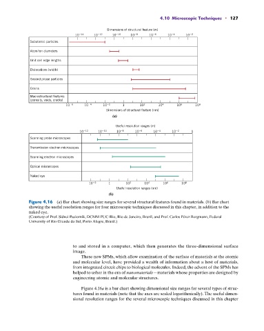
4.10 Microscopic Techniques  •  127


                                                Dimensions of structural feature (m)
                                  10  14  10  12  10  10  10  8   10  6   10  4   10  2
              Subatomic particles

              Atom/ion diameters
              Unit cell edge lengths

              Dislocations (width)
              Second phase particles

              Grains
              Macrostructural features
              (porosity, voids, cracks)
                              10  6   10  4   10  2   1       10 2    10 4    10 6    10 8
                                               Dimensions of structural feature (nm)
                                                  (a)

                                                   Useful resolution ranges (m)
                                    10  12  10  10  10  8   10  6   10  4   10  2   1
              Scanning probe microscopes

              Transmission electron microscopes
              Scanning electron microscopes

              Optical microscopes

              Naked eye
                                        10  2   1       10 2    10 4    10 6    10 8
                                                    Useful resolution ranges (nm)
                                                (b)
              Figure 4.16  (a) Bar chart showing size ranges for several structural features found in materials. (b) Bar chart
              showing the useful resolution ranges for four microscopic techniques discussed in this chapter, in addition to the
              naked eye.
              (Courtesy of Prof. Sidnei Paciornik, DCMM PUC-Rio, Rio de Janeiro, Brazil, and Prof. Carlos Pérez Bergmann, Federal
              University of Rio Grande do Sul, Porto Alegre, Brazil.)


                                 to and stored in a computer, which then generates the three-dimensional surface
                                 image.
                                    These new SPMs, which allow examination of the surface of materials at the atomic
                                 and molecular level, have provided a wealth of information about a host of materials,
                                 from integrated circuit chips to biological molecules. Indeed, the advent of the SPMs has
                                 helped to usher in the era of nanomaterials—materials whose properties are designed by
                                 engineering atomic and molecular structures.

                                    Figure 4.16a is a bar chart showing dimensional size ranges for several types of struc-
                                 tures found in materials (note that the axes are scaled logarithmically). The useful dimen-
                                 sional resolution ranges for the several microscopic techniques discussed in this chapter