
Page 153 - Materials Science and Engineering An Introduction
P. 153
4.10 Microscopic Techniques • 125
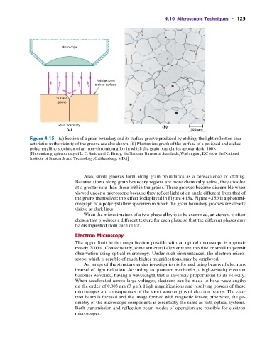
Microscope
Polished and
etched surface
Surface
groove
Grain boundary (b)
(a)
Figure 4.15 (a) Section of a grain boundary and its surface groove produced by etching; the light reflection char-
acteristics in the vicinity of the groove are also shown. (b) Photomicrograph of the surface of a polished and etched
polycrystalline specimen of an iron–chromium alloy in which the grain boundaries appear dark, 100 .
[Photomicrograph courtesy of L. C. Smith and C. Brady, the National Bureau of Standards, Washington, DC (now the National
Institute of Standards and Technology, Gaithersburg, MD.)]
Also, small grooves form along grain boundaries as a consequence of etching.
Because atoms along grain boundary regions are more chemically active, they dissolve
at a greater rate than those within the grains. These grooves become discernible when
viewed under a microscope because they reflect light at an angle different from that of
the grains themselves; this effect is displayed in Figure 4.15a. Figure 4.15b is a photomi-
crograph of a polycrystalline specimen in which the grain boundary grooves are clearly
visible as dark lines.
When the microstructure of a two-phase alloy is to be examined, an etchant is often
chosen that produces a different texture for each phase so that the different phases may
be distinguished from each other.
Electron Microscopy
The upper limit to the magnification possible with an optical microscope is approxi-
mately 2000 . Consequently, some structural elements are too fine or small to permit
observation using optical microscopy. Under such circumstances, the electron micro-
scope, which is capable of much higher magnifications, may be employed.
An image of the structure under investigation is formed using beams of electrons
instead of light radiation. According to quantum mechanics, a high-velocity electron
becomes wavelike, having a wavelength that is inversely proportional to its velocity.
When accelerated across large voltages, electrons can be made to have wavelengths
on the order of 0.003 nm (3 pm). High magnifications and resolving powers of these
microscopes are consequences of the short wavelengths of electron beams. The elec-
tron beam is focused and the image formed with magnetic lenses; otherwise, the ge-
ometry of the microscope components is essentially the same as with optical systems.
Both transmission and reflection beam modes of operation are possible for electron
microscopes.