
Page 126 - Materials Chemistry, Second Edition
P. 126
113
2.4. The Amorphous State
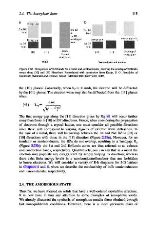
Figure 2.78. Comparison of 2-D bands for a metal and semiconductor, showing the overlap of Brillouin
zones along [10] and [11] directions. Reproduced with permission from Kasap, S. O. Principles of
Electronic Materials and Devices, 3rd ed., McGraw-Hill: New York, 2006.
the {10} planes. Conversely, when k y ¼ np/b, the electron will be diffracted
by the {01} planes. The electron wave may also be diffracted from the {11} planes
when:
np
ð41Þ k xy ¼ q ffiffiffiffiffiffiffiffiffiffiffiffiffiffiffiffiffiffiffiffi
2
2 a þb 2
b
4
The first energy gap along the [11] direction given by Eq. 41 will occur farther
away than those in [10] or [01] directions. Hence, when considering the propagation
of electrons through a crystal lattice, one must consider all possible directions
since these will correspond to varying degrees of electron wave diffraction. In
the case of a metal, there will be overlap between the 1st and 2nd BZ in [01] or
[10] directions with those in the [11] direction (Figure 2.78a). However, for an
insulator or semiconductor, the BZs do not overlap, resulting in a bandgap, E g
(Figure 2.78b); the 1st and 2nd Brillouin zones are thus referred to as valence
and conduction bands, respectively. Qualitatively, one can say that in a metal the
electron may populate any energy level by simply varying its direction, whereas
there exist finite energy levels in a semiconductor/insulator that are forbidden
to house electrons. We will consider a variety of E-k diagrams for 3-D lattices
in Chapters 4 and 6, when we describe the conductivity of bulk semiconductors
and nanomaterials, respectively.
2.4. THE AMORPHOUS STATE
Thus far, we have focused on solids that have a well-ordered crystalline structure.
It is now time to turn our attention to some examples of amorphous solids.
We already discussed the synthesis of amorphous metals; those obtained through
fast nonequilibrium conditions. However, there is a more pervasive class of