
Page 407 - Mechatronics for Safety, Security and Dependability in a New Era
P. 407
Ch79-I044963.fm Page 391 Saturday, July 29, 2006 7:14 AM
Page 391
7:14 AM
Ch79-I044963.fm
Saturday, July 29, 2006
391
391
Vout
R1 L1
Vias
Stubi
T L 4
High band rectifier l«
Antenna -TL3 Low band rectifier
Stub2
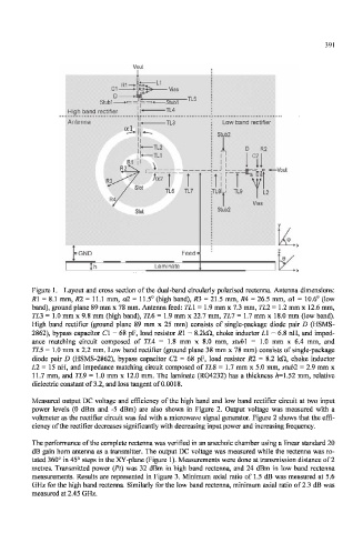
Figure 1. Layout and cross section of the dual-band circularly polarised rectenna. Antenna dimensions:
R\ = 8.1 mm, R2 = 11.1 mm, til = 11.5° (high band), #3 = 21.5 mm, RA = 26.5 mm, a\ = 10.6° (low
band), ground plane 89 mm x 78 mm. Antenna feed: 7X1 = 1.9 mm x 7.3 mm, 7X2 = 1.2 mm x 12.6 mm,
7X3 = 1.0 mm x 9.8 mm (high band), 7X6 = 1.9 mm x 22.7 mm, 7X7 = 1.7 mm x 18.0 mm (low band).
High band rectifier (ground plane 89 mm x 25 mm) consists of single-package diode pair D (HSMS-
2862), bypass capacitor C\ = 68 pF, load resistor R\ = 8.2kQ, choke inductor XI = 6.8 nH, and imped-
ance matching circuit composed of XX4 = 1.8 mm x 8.0 mm, stub\ = 1.0 mm x 6.4 mm, and
7X5 = 1.0 mm x 2.2 mm. Low band rectifier (ground plane 38 mm x 78 mm) consists of single-package
diode pair D (HSMS-2862), bypass capacitor C2 = 68 pF, load resistor R2 = 8.2 kD, choke inductor
X2 = 15 nH, and impedance matching circuit composed of XX8 = 1.7 mm x 5.0 mm, stub! = 2.9 mm x
11.7 mm, and 7X9 = 1.0 mm x 12.0 mm. The laminate (RO4232) has a thickness h=l.52 mm, relative
dielectric constant of 3.2, and loss tangent of 0.0018.
Measured output DC voltage and efficiency of the high band and low band rectifier circuit at two input
power levels (0 dBm and -5 dBm) are also shown in Figure 2. Output voltage was measured with a
voltmeter as the rectifier circuit was fed with a microwave signal generator. Figure 2 shows that the effi-
ciency of the rectifier decreases significantly with decreasing input power and increasing frequency.
The performance of the complete rectenna was verified in an anechoic chamber using a linear standard 20
dB gain horn antenna as a transmitter. The output DC voltage was measured while the rectenna was ro-
tated 360° in 45° steps in the XY-plane (Figure 1). Measurements were done at transmission distance of 2
metres. Transmitted power (Pt) was 32 dBm in high band rectenna, and 24 dBm in low band rectenna
measurements. Results are represented in Figure 3. Minimum axial ratio of 1.5 dB was measured at 5.6
GHz for the high band rectenna. Similarly for the low band rectenna, minimum axial ratio of 2.3 dB was
measured at 2.45 GHz.