
Page 409 - Mechatronics for Safety, Security and Dependability in a New Era
P. 409
Ch79-I044963.fm Page 393 Saturday, July 29, 2006 7:14 AM
Saturday, July 29, 2006
7:14 AM
Page 393
Ch79-I044963.fm
393
393
DUAL-BAND CP ANTENNA WITH EBG STRUCTURE
In order to reduce electromagnetic propagation from the proposed rectenna at certain frequencies, the ef-
fect of introducing a 2D EBG structure to the ground plane of the antenna was studied. The layout of the
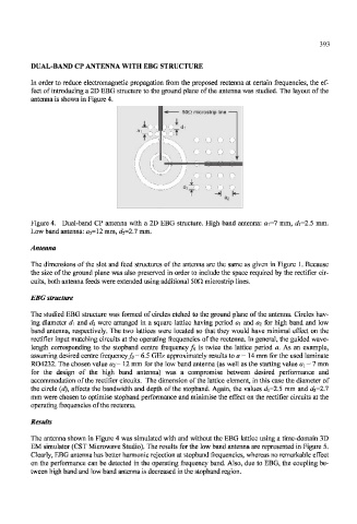
antenna is shown in Figure 4.
-« 50n microstrip line —
) -A
a i ':-•[':-' d1
:;>, o o o o
^—Mi
T -H K-
a2
Figure 4. Dual-band CP antenna with a 2D EBG structure. High band antenna: ai=7 mm, di=2.5 mm.
Low band antenna: a 2=\2 mm, d 2=2J mm.
The dimensions of the slot and feed structures of the antenna are the same as given in Figure 1. Because
the size of the ground plane was also preserved in order to include the space required by the rectifier cir-
cuits, both antenna feeds were extended using additional 50Q microstrip lines.
EBG structure
The studied EBG structure was formed of circles etched to the ground plane of the antenna. Circles hav-
ing diameter d\ and d 2 were arranged in a square lattice having period a\ and a 2 for high band and low
band antenna, respectively. The two lattices were located so that they would have minimal effect on the
rectifier input matching circuits at the operating frequencies of the rectenna. In general, the guided wave-
length corresponding to the stopband centre frequency fi> is twice the lattice period a. As an example,
assuming desired centre frequency fg= 6.5 GHz approximately results to a = 14 mm for the used laminate
RO4232. The chosen value a 2 = 12 mm for the low band antenna (as well as the starting value a\ = l mm
for the design of the high band antenna) was a compromise between desired performance and
accommodation of the rectifier circuits. The dimension of the lattice element, in this case the diameter of
the circle (d), affects the bandwidth and depth of the stopband. Again, the values di=2.5 mm and d 2=2.1
mm were chosen to optimise stopband performance and minimise the effect on the rectifier circuits at the
operating frequencies of the rectenna.
Results
The antenna shown in Figure 4 was simulated with and without the EBG lattice using a time-domain 3D
EM simulator (CST Microwave Studio). The results for the low band antenna are represented in Figure 5.
Clearly, EBG antenna has better harmonic rejection at stopband frequencies, whereas no remarkable effect
on the performance can be detected in the operating frequency band. Also, due to EBG, the coupling be-
tween high band and low band antenna is decreased in the stopband region.