
Page 14 -
P. 14
1.2 Fabrication Methods 3
(a) Undercut Mask (b)
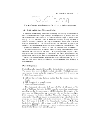
Fig. 1.1. Isotropic (a)and anisotropic (b)etchings for bulk micromachining
1.2.1 Bulk and Surface Micromachining
To fabricate structures by bulk micromachining, two etching methods can be
used, isotropic and anisotropic etchings. In isotropic etching, etching proceeds
at the same rate in all directions, which leads to the isotropic undercut shown
in Fig. 1.1a. On the other hand, in anisotropic etching, etching proceeds at
different rates dependingon the crystal orientation, which leads to precise
features, shown in Fig. 1.1b. Silicon V-grooves are fabricated by anisotropic
etchingof a (100) silicon substrate and are widely used in optical MEMS. The
V-grooves are also used in packing of fiber and optoelectronic components.
To fabricate structures by surface micromachining, a sacrificed film is first
deposited and patterned on the wafer. The film to be formed into the desired
microstructure is next deposited and patterned, and the sacrificed layer is then
etched away, undercuttingthe microstructure and leavingit freely suspended.
There are two kinds of surface micromachining: photolithography for a thick-
ness less than several 10 µm, and electron beam lithography for a thickness of
less than 1 µm.
Photolithography
Photolithography is most widely used for the fabrication of a microstructure.
The process steps shown in Fig. 1.2 include ultraviolet (UV) light exposure,
development, etching, and resist stripping. This essentially 2-D process has
the followingcharacteristics:
1. difficulty in fabricatingfeatures smaller than the exposure light wave-
length
2. high throughput by a mask process
3. relatively high aspect ratio.
The electrostatic micromotor [1.2] shown in Fig. 1.3, fabricated by Fan
et al. of California University in 1988, caused a tremendous sensation and
paved the way for the development of MEMS technology. The diameter of the
microrotor was 120 µm and the gap between the rotor and the stator was 2 µm.
Both were made of polysilicon thin films. When pulse voltages are applied to
stator poles with different phases, an electrostatic torque arises between the
rotor and the stator, which leads to the rotation rate of 500 rpm. Two years
later, Mehregany et al. [1.22] of the Massachusetts Institute of Technology
fabricated a micromotor with a higher speed of 15000 rpm. Recently, com-
mercially used MEMS such as pressure sensors, accelerometers, and gyros are
fabricated by the successive photolithography.