Page 16 -
P. 16

1.2 Fabrication Methods   5
                                             (a)
                                                              SiO 2
                                                          GaAs substrate

                                                 C F  ion beam  SiO 2
                                                  3 8
                                             (b)
                                                          GaAs substrate


                                                               H SO +H O +H O
                                                                      2
                                                                        2
                                                                   4
                                                                2
                                                                          2
                                             (c)        SiO 2
                                                         GaAs substrate
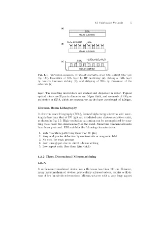
                            Fig. 1.4. Fabrication sequence, by photolithography, of an SiO 2 optical rotor (see
                            Fig. 1.26). Deposition of SiO 2 layer by RF sputtering (a), etching of SiO 2 layer
                            by reactive ion-beam etching (b), and stripping of SiO 2 by dissolution of the
                            substrate (c)


                            layer. The resultingmicrorotors are washed and dispersed in water. Typical
                            optical rotors are 20 µm in diameter and 10 µm thick, and are made of SiO 2 or
                            polyimide or SU-8, which are transparent at the laser wavelength of 1.06 µm.


                            Electron Beam Lithography
                            In electron beam lithography (EBL), focused high-energy electrons with wave-
                            lengths less than that of UV light are irradiated onto electron-sensitive resist,
                            as shown in Fig. 1.5. High-resolution patterning can be accomplished by scan-
                            ningthe e-beam two-dimensionally on the resist. Numerous commercial resists
                            have been produced. EBL exhibits the followingcharacteristics:

                             1. high-resolution patterning (less than 0.1 µm)
                             2. Easy and precise deflection by electrostatic or magnetic field
                             3. No need for mask process
                             4. Low throughput due to direct e-beam writing
                             5. Low aspect ratio (less than 1 µmthick).


                            1.2.2 Three-Dimensional Micromachining

                            LIGA

                            A surface-micromachined device has a thickness less than 100 µm. However,
                            many micromechanical devices, particularly microactuators, require a thick-
                            ness of few hundreds micrometers. Microstructures with a very large aspect
   11   12   13   14   15   16   17   18   19   20   21