
Page 21 -
P. 21
10 1 From Optical MEMS to Micromechanical Photonics
absorption rate is proportional to the square of the incident light intensity, a
3-D structure is fabricated by scanningthe focused spot of a near-infrared-
wavelength beam in three dimensions inside the resin. The lateral and depth
resolutions are said to 0.62 and 2.2 µm, respectively. After that, they also
succeeded in fabricatinga micrometer sized cow with a resolution of 140 nm
[1.30].
Replication
Replication from a mold is important technology for realizing lower cost and
mass production. For optical MEMS applications, the use of sol–gels which
become glass-like material upon curing is foreseen. ORMOCER US-S4 is such
a material. It is optically transparent over the wavelength from 400 to 1600 nm
and has a refractive index of 1.52 at 588 nm. Obi et al. replicated many sol–gel
micro-optical devices and optical MEMS includinga sol–gel cantilever with a
microlens on the top [1.31].
1.2.3 Monolithic Integration – Micromachining for an LD
Monolithic integration of micromechanics is possible not only on a Si sub-
strate but also on a semiconductor LD substrate of GaAs [1.14] or InP [1.15].
A smooth etched surface and a deep vertical sidewall are necessary for good
lasingcharacteristics of LDs.
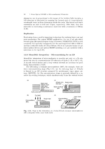
For fabricatinga resonant microcantilever (MC), for example, there are
three micromachiningsteps (Fig. 1.11). (a) An etch-stop layer of AlGaAs
is formed in an LD structure prepared by metalorganic vapor phase epi-
taxy (MOVPE). (b) The microstructure shape is precisely defined by a re-
active dry-etchingtechnique, which simultaneously forms the vertical etched
(a) (c)
AlGaAs etch- Resist mask
GaAs (cap) stop layer
AlGaAs (clad)
Active layer GaAs sacrificial
AlGaAs (clad) part
GaAs
AlGaAs (etch-stop layer) GaAs substrate
GaAs substrate
(b) Cl beam (d)
2
Laser diode
Resist mask Microcantilever (LD)
Microcantilever Etched mirror (MC)
(MC)
GaAs substrate
GaAs substrate
Fig. 1.11. Steps in the fabrication of a GaAs/AlGaAs resonant microcantilever
(MC)integrated with a laser diode (LD)