Page 15 -
P. 15

4     1 From Optical MEMS to Micromechanical Photonics
                                                                 Al (sacrificed layer)
                                                                 Si substrate
                                                                 Resist


                                                                Exposure (UV light)


                                                                 Mask


                                                                 Development


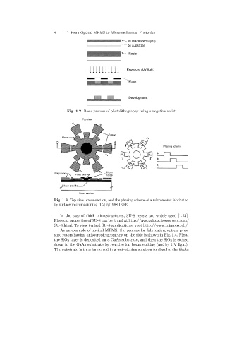
                                  Fig. 1.2. Basic process of photolithography using a negative resist

                                          Top view
                                     F 2
                                                   F 1

                                                       Stators
                                Rotor
                                                                          +V
                             A                            A 9    F 2    F 1
                                                                   T 9  T
                                                                                  Phasing scheme
                                                                            9  F 1
                                                     F 3     F 3           F 3
                                                                               F 2
                                                                   T  T 9      F 3
                                                                  9     F 9
                                                             + - V  F 1  2
                                         F 1
                                                  F 2  Silicon
                            Polysilicon
                                      Fixed axle      nitride
                                Silicon dioxidie
                                        Cross section
                            Fig. 1.3. Top view, cross-section, and the phasing scheme of a micromotor fabricated
                            by surface micromachining [1.2] c  1988 IEEE

                               In the case of thick microstructures, SU-8 resists are widely used [1.23].
                            Physical properties of SU-8 can be found at http://aveclafaux.freeservers.com/
                            SU-8.html. To view typical SU-8 applications, visit http://www.mimotec.ch/.
                               As an example of optical MEMS, the process for fabricatingoptical pres-
                            sure rotors having anisotropic geometry on the side is shown in Fig. 1.4. First,
                            the SiO 2 layer is deposited on a GaAs substrate, and then the SiO 2 is etched
                            down to the GaAs substrate by reactive ion beam etching(not by UV light).
                            The substrate is then immersed in a wet-etchingsolution to dissolve the GaAs
   10   11   12   13   14   15   16   17   18   19   20