
Page 193 - A Practical Guide from Design Planning to Manufacturing
P. 193
166 Chapter Five
ready. This means that the uops are no longer in the original program
order. Uops can dispatch before older uops if their sources are ready first.
When a uop is dispatched, its destination register and minimum latency
are used to update the scoreboard showing which registers have ready
data. This means that dependent uops may be scheduled too soon if a
uop takes longer than expected, for instance if a load misses in the cache.
Uops that are scheduled too soon will have to be replayed, going through
dispatch again to receive their correct source data. The Pentium 4 can
dispatch a maximum of 6 uops in one cycle.
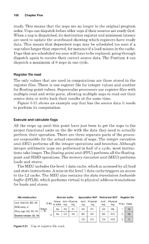
Register file read
The only values that are used in computations are those stored in the
register files. There is one register file for integer values and another
for floating-point values. Superscalar processors use register files with
multiple read and write ports, allowing multiple uops to read out their
source data or write back their results at the same time.
Figure 5-21 shows an example uop that has the source data it needs
to perform its computation.
Execute and calculate flags
All the steps up until this point have just been to get the uops to the
proper functional units on the die with the data they need to actually
perform their operation. There are three separate parts of the proces-
sor responsible for the actual execution of uops. The integer execution
unit (IEU) performs all the integer operations and branches. Although
integer arithmetic uops are performed in half of a cycle, most instruc-
tions take longer. The floating-point unit (FPU) performs all the floating-
point and SIMD operations. The memory execution unit (MEU) performs
loads and stores.
The MEU includes the level 1 data cache, which is accessed by all load
and store instructions. A miss in the level 1 data cache triggers an access
to the L2 cache. The MEU also contains the data translation lookaside
buffer (DTLB), which performs virtual to physical address translations
for loads and stores.
Microinstruction Reorder buffer Speculative RAT Retirement RAT Register file
Ready Arch Physical Arch Physical Arch Physical
Uop: Add CX, BX, AX Entry to retire reg reg reg reg reg reg Entry Value
ROB entry: 2
Oldest 1 No AX R1 AX R1 AX R8 1 16
Phys regs: R3, R2, R1
2 No CX R3 BX R2 BX R12 2 33
Source values: 33, 16
CX R3 CX R15 3 5
Figure 5-21 Uop at register file read.