
Page 43 - A Practical Guide from Design Planning to Manufacturing
P. 43
The Evolution of the Microprocessor 19
Transistor scaling
The reason smaller transistors switch faster is that although they draw
less current, they also have less capacitance. Less charge has to be
moved to switch their gates on and off. The delay of switching a gate
(T DELAY ) is determined by the capacitance of the gate (C GATE ), the total
voltage swing (V ), and the drain to source current (I ) drawn by the
DS
dd
transistor causing the gate to switch.
V
T ∝ C × dd
DELAY GATE
I
DS
Higher capacitance or higher voltage requires more charge to be
drawn out of the gate to switch the transistor, and therefore more cur-
rent to switch in the same amount of time. The capacitance of the gate
increases linearly with the width (W) and length (L) of the gate and
decreases linearly with the thickness of the gate oxide (T ).
OX
V W × L V
T ∝ C × dd ∝ × dd
DELAY GATE
I T I
DS OX DS
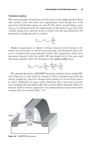
The current drawn by a MOSFET increases with the device width (W),
since there is a wider path for charges to flow, and decreases with the
device length (L), since the charges have farther to travel from source
) increases current,
to drain. Reducing the gate oxide thickness (T OX
since pushing the gate physically closer to the silicon channel allows its
electric field to better penetrate the semiconductor and draw more
charges into the channel (Fig. 1-8).
Poly
gate
Width
T OX
Source Drain
Length
Figure 1-8 MOSFET dimensions.