
Page 44 - A Practical Guide from Design Planning to Manufacturing
P. 44
20 Chapter One
To draw any current at all, the gate voltage must be greater than a
certain minimum voltage called the threshold voltage (V T ). This volt-
age is determined by both the gate oxide thickness and the concentra-
tion of dopant atoms added to the channel. Current from the drain to
source increases quadratically after the threshold voltage is crossed. The
current of MOSFETs is discussed in more detail in Chap. 7.
I ∝ W × ( V − V ) 2
×
DS dd T
LT
OX
Putting together these equations for delay and current we find:
V
2
T ∝ L × dd
DELAY 2
( V − V )
dd T
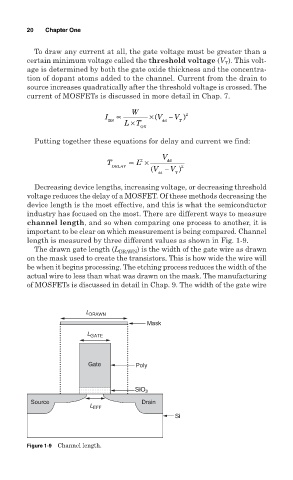
Decreasing device lengths, increasing voltage, or decreasing threshold
voltage reduces the delay of a MOSFET. Of these methods decreasing the
device length is the most effective, and this is what the semiconductor
industry has focused on the most. There are different ways to measure
channel length, and so when comparing one process to another, it is
important to be clear on which measurement is being compared. Channel
length is measured by three different values as shown in Fig. 1-9.
The drawn gate length (L DRAWN ) is the width of the gate wire as drawn
on the mask used to create the transistors. This is how wide the wire will
be when it begins processing. The etching process reduces the width of the
actual wire to less than what was drawn on the mask. The manufacturing
of MOSFETs is discussed in detail in Chap. 9. The width of the gate wire
L DRAWN
Mask
L GATE
Gate Poly
SiO 2
Source Drain
L EFF
Si
Figure 1-9 Channel length.