
Page 73 - A Practical Guide from Design Planning to Manufacturing
P. 73
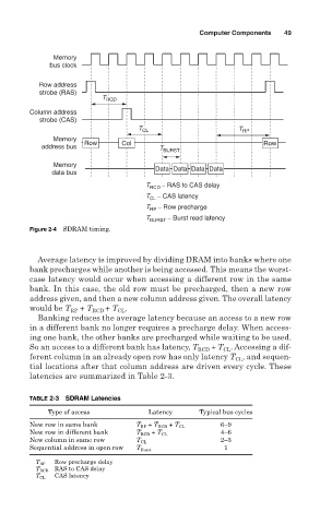
Computer Components  49


              Memory
             bus clock

           Row address
           strobe (RAS)
                          T RCD
        Column address
           strobe (CAS)
                                   T CL                     T RP
              Memory
           address bus  Row    Col      T BURST                   Row

              Memory
              data bus                 Data Data Data Data
                                     T RCD − RAS to CAS delay
                                     T CL  − CAS latency
                                     T RP  − Row precharge
                                     T BURST  − Burst read latency
        Figure 2-4 SDRAM timing.


          Average latency is improved by dividing DRAM into banks where one
        bank precharges while another is being accessed. This means the worst-
        case latency would occur when accessing a different row in the same
        bank. In this case, the old row must be precharged, then a new row
        address given, and then a new column address given. The overall latency
        would be T RP  + T RCD  + T .
                              CL
          Banking reduces the average latency because an access to a new row
        in a different bank no longer requires a precharge delay. When access-
        ing one bank, the other banks are precharged while waiting to be used.
        So an access to a different bank has latency, T RCD  + T . Accessing a dif-
                                                        CL
        ferent column in an already open row has only latency T , and sequen-
                                                           CL
        tial locations after that column address are driven every cycle. These
        latencies are summarized in Table 2-3.

        TABLE 2-3  SDRAM Latencies

             Type of access           Latency     Typical bus cycles
        New row in same bank       T RP + T RCD + T CL  6–9
        New row in different bank  T RCD + T CL         4–6
        New column in same row     T CL                 2–3
        Sequential address in open row  T Burst          1
               Row precharge delay
          T RP
          T RCD  RAS to CAS delay
               CAS latency
          T CL