
Page 102 - Microsensors, MEMS and Smart Devices - Gardner Varadhan and Awadelkarim
P. 102
MONOLITHIC PROCESSING 83
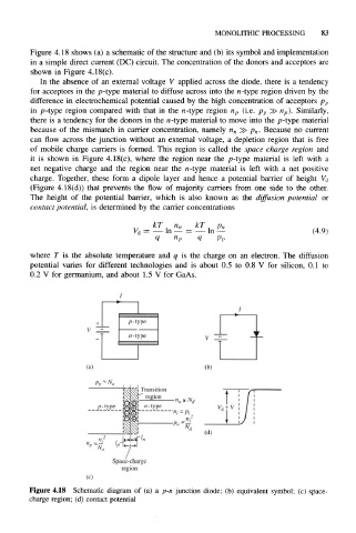
Figure 4.18 shows (a) a schematic of the structure and (b) its symbol and implementation
in a simple direct current (DC) circuit. The concentration of the donors and acceptors are
shown in Figure 4.18(c).
In the absence of an external voltage V applied across the diode, there is a tendency
for acceptors in the p-type material to diffuse across into the n-type region driven by the
difference in electrochemical potential caused by the high concentration of acceptors p p
in p-type region compared with that in the n-type region n p (i.e. p p » n p). Similarly,
there is a tendency for the donors in the n-type material to move into the p-type material
because of the mismatch in carrier concentration, namely n n >> p n. Because no current
can flow across the junction without an external voltage, a depletion region that is free
of mobile charge carriers is formed. This region is called the space charge region and
it is shown in Figure 4.18(c), where the region near the p-type material is left with a
net negative charge and the region near the n-type material is left with a net positive
charge. Together, these form a dipole layer and hence a potential barrier of height V d
(Figure 4.18(d)) that prevents the flow of majority carriers from one side to the other.
The height of the potential barrier, which is also known as the diffusion potential or
contact potential, is determined by the carrier concentrations
(4.9)
q P P
where T is the absolute temperature and q is the charge on an electron. The diffusion
potential varies for different technologies and is about 0.5 to 0.8 V for silicon, 0.1 to
0.2 V for germanium, and about 1.5 V for GaAs.
p-type
n-type
aia^i^fijggg;'^
(a)
(d)
Space-charge
region
Figure 4.18 Schematic diagram of (a) a p-n junction diode; (b) equivalent symbol; (c) space-
charge region; (d) contact potential