
Page 105 - Microsensors, MEMS and Smart Devices - Gardner Varadhan and Awadelkarim
P. 105
86 STANDARD MICROELECTRONIC TECHNOLOGIES
shown in Figure 4.19. The threshold voltage V T of a typical silicon junction diode is
0.6 V and has a linear temperature coefficient of about —1.7 mV/°C at 20 °C. Therefore,
operating a diode at constant current in the forward-bias regime produces a simple and
linear temperature sensor.
The BJT consists of either a p-type region sandwiched between two n-type regions
for an n-p-n transistor or an n-type region sandwiched between two p-type regions for
a p-n-p transistor; hence, it could be regarded as an n-p and p-n diode back to back.
In the last section, we saw how a bipolar process can be used to fabricate a vertical
n-p-n transistor and lateral p-n-p transistor for an IC. All the transistor voltages and
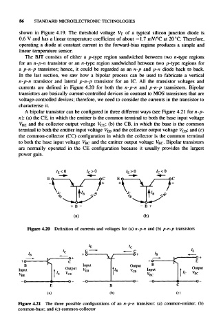
currents are defined in Figure 4.20 for both the n-p-n and p-n-p transistors. Bipolar
transistors are basically current-controlled devices in contrast to MOS transistors that are
voltage-controlled devices; therefore, we need to consider the currents in the transistor to
characterise it.
A bipolar transistor can be configured in three different ways (see Figure 4.21 for n-p-
n): (a) the CE, in which the emitter is the common terminal to both the base input voltage
and the collector output voltage V CE; (b) the CB, in which the base is the common
V BE
terminal to both the emitter input voltage VEB and the collector output voltage V CB; and (c)
the common-collector (CC) configuration in which the collector is the common terminal
to both the base input voltage V BC and the emitter output voltage V EC- Bipolar transistors
are normally operated in the CE configuration because it usually provides the largest
power gain.
I E <0 I c >0 I E >0 I c <0
Figure 4.20 Definition of currents and voltages for (a) n-p-n and (b) p-n-p transistors
E C E
I C
IT L r
C K
B Input Output B
Input Output B V CB Input Output
I E V CE I c V EC
V BE V BC
E B C
(a) (b) (c)
Figure 4.21 The three possible configurations of an n-p-n transistor: (a) common-emitter; (b)
common-base; and (c) common-collector