
Page 109 - Microsensors, MEMS and Smart Devices - Gardner Varadhan and Awadelkarim
P. 109
90 STANDARD MICROELECTRONIC TECHNOLOGIES
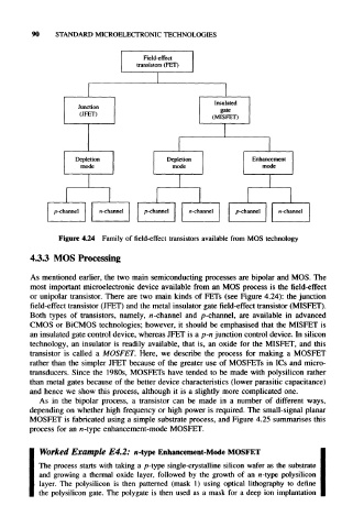
Figure 4.24 Family of field-effect transistors available from MOS technology
4.3.3 MOS Processing
As mentioned earlier, the two main semiconducting processes are bipolar and MOS. The
most important microelectronic device available from an MOS process is the field-effect
or unipolar transistor. There are two main kinds of FETs (see Figure 4.24): the junction
field-effect transistor (JFET) and the metal insulator gate field-effect transistor (MISFET).
Both types of transistors, namely, n -channel and p-channel, are available in advanced
CMOS or BiCMOS technologies; however, it should be emphasised that the MISFET is
an insulated gate control device, whereas JFET is a p-n junction control device. In silicon
technology, an insulator is readily available, that is, an oxide for the MISFET, and this
transistor is called a MOSFET. Here, we describe the process for making a MOSFET
rather than the simpler JFET because of the greater use of MOSFETs in ICs and micro-
transducers. Since the 1980s, MOSFETs have tended to be made with polysilicon rather
than metal gates because of the better device characteristics (lower parasitic capacitance)
and hence we show this process, although it is a slightly more complicated one.
As in the bipolar process, a transistor can be made in a number of different ways,
depending on whether high frequency or high power is required. The small-signal planar
MOSFET is fabricated using a simple substrate process, and Figure 4.25 summarises this
process for an n-type enhancement-mode MOSFET.
Worked Example E4.2: n-type Enhancement-Mode MOSFET
The process starts with taking a p-type single-crystalline silicon wafer as the substrate
and growing a thermal oxide layer, followed by the growth of an n-type polysilicon
layer. The polysilicon is then patterned (mask 1) using optical lithography to define
the polysilicon gate. The polygate is then used as a mask for a deep ion implantation