
Page 111 - Microsensors, MEMS and Smart Devices - Gardner Varadhan and Awadelkarim
P. 111
92 STANDARD MICROELECTRONIC TECHNOLOGIES
Channel
Remove mask, implant
p-type substrate
whole with n+
Grow SiO, Remove nitride
Grow silicon nitride Poly over wafer
Mask and etch poly
Mask for gate
Ion-implant with light
Etch nitride, leaving gate
Metalize contacts for
Mask drain area, overlap gate, source, gate, and
implant p-doped channel
drain
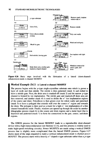
Figure 4.26 Basic steps involved with the fabrication of a lateral (short-channel)
enhancement-mode n -channel MOSFET
Worked Example E4.3: A Lateral n-channel MOSFET
The process begins with the p-type single-crystalline substrate onto which is grown a
layer of oxide and then nitride. The nitride is then patterned (mask 1) and etched to
leave a nitride gate. Next, the drain area is masked off (mask 2) and the narrow p-type
channel is formed by ion implantation. The nitride gate and masked-off drain area are
then removed, and another mask (4) is used to define the n + ion implantation regions
of the source and drain. Polysilicon is then grown over the whole wafer and patterned
(mask 5) to leave a polygate that extends well over the source n + region and towards
the drain. The polygate is then used as a mask for a light n – ion implantation of a thin
channel beneath the oxide. Finally, windows are opened up through the oxide by another
lithographic process (mask 6) to the source and drain regions and a metal layer that is
deposited and patterned (mask 7) to form the connections to the gate, source, and drain
regions.
The DMOS process for the lateral MOSFET leads to a reproducible short-channel
device with a high transconductance (see Section 4.3.4), and this process is widely used to
make high-speed switching circuitry. Power MOSFETs are made using a vertical DMOS
process that is slightly more complicated than the lateral DMOS process. Figure 4.27
shows most of the steps required to make a vertical enhancement-mode n-channel power
+
MOSFET. The process starts with a heavily n -doped n-type substrate rather than a p-type