
Page 115 - Microsensors, MEMS and Smart Devices - Gardner Varadhan and Awadelkarim
P. 115
96 STANDARD MICROELECTRONIC TECHNOLOGIES
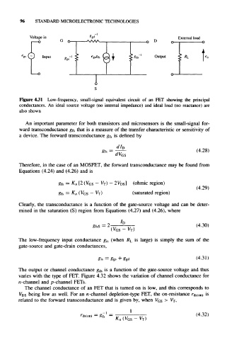
Voltage in External load
O—I O
Output R L
Figure 4.31 Low-frequency, small-signal equivalent circuit of an FET showing the principal
conductances. An ideal source voltage (no internal impedance) and ideal load (no reactance) are
also shown
An important parameter for both transistors and microsensors is the small-signal for-
ward transconductance g fs that is a measure of the transfer characteristic or sensitivity of
a device. The forward transconductance g fs is defined by
I
d D
(4.28)
Therefore, in the case of an MOSFET, the forward transconductance may be found from
Equations (4.24) and (4.26) and is
= K n [2 (V GS - V T) ~ 2V DS] (ohmic region)
g fs
(4.29)
K
gk = n (V Gs - W) (saturated region)
Clearly, the transconductance is a function of the gate-source voltage and can be deter-
mined in the saturation (S) region from Equations (4.27) and (4.26), where
gf s s = 2 (4.30)
(V GS - V T)
The low-frequency input conductance g- ls (when R L is large) is simply the sum of the
gate-source and gate-drain conductances,
g is = g gs + (4.31)
The output or channel conductance g ds is a function of the gate-source voltage and thus
varies with the type of FET. Figure 4.32 shows the variation of channel conductance for
n-channel and p-channel FETs.
The channel conductance of an FET that is turned on is low, and this corresponds to
V DS being low as well. For an n-channel depletion-type FET, the on-resistance r ds(on) is
related to the forward transconductance and is given by, when V GS > V T,
1
r (4.32)
ds(on) — g fs —
K n (V GS - V T)