
Page 117 - Microsensors, MEMS and Smart Devices - Gardner Varadhan and Awadelkarim
P. 117
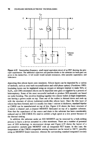
98    STANDARD MICROELECTRONIC TECHNOLOGIES


                 G  •-                                      -• D


                                                           Substrate
                                                            effect


  Figure 4.33  Intermediate-frequency,  small-signal equivalent circuit of an FET showing the prin-
  cipal capacitances. The additional capacitors and junction diodes to the substrate (or back-gate) are
   given  in  the  dashed  box. A  full  model  would  include  resistances,  other  parasitic capacitance,  and
   inductance

  depositing  thin silicon  layers  onto  insulators.  Silicon  layers can be deposited  by a variety
  of methods,  such as zone-melt recrystallisation  and solid-phase epitaxy (Furukawa 1985).
  Insulating  layers can be  implanted using an oxygen or nitrogen implant to  make SiO 2  or
  Si3N 4, and (l00)-orientated  silicon can be deposited onto glass or sapphire by a process of
  heteroepitaxy.  Some  of  the  most  successful  methods  to produce  SOI presently  are  based
  on wafer bonding. This involves bonding together  two silicon  wafers at high temperature,
  one  having  a  grown oxide  on top.  Then  one  of  the  wafers  is thinned down and  ends up
  with  the  structure of  silicon  (substrate)-oxide-thin  silicon  layer. Once  the  thin  layer of
  silicon  has been formed, and it is usually less than  1 micron in thickness,  standard bipolar
  or  CMOS  can  be  manufactured on  top  of  this.  Figure 4.34  shows  the  basic  structure of
  a  lateral  n-channel and  p-channel  MOSFET  fabricated  on  top  of  a  sapphire  substrate.
  Note that the  capacitance of  the  source  and drain to  the  substrate has  been considerably
  reduced  and  so  SOI  CMOS  ICs tend to exhibit  a  high  speed  at  a  low power because of
  the thermal  sinking.
     In  addition,  the  substrate  under  an  SOI  MOSFET  can  be  removed  by a bulk-etching
  process  to  leave a device mounted in a thin  membrane. There  are a number of potential
  uses  of  SOI  technology  in  microsensor  design  and  Figure 4.35  shows  the  layout  of  a
  gas-sensitive  catalytic-gate  MOSFET  with  an  integrated  FET  heater.  In  this  case,  the
  temperature of the CMOS-compatible  sensing transistor  can be raised  to  180°C,  possibly
  using an MOSFET heater transistor, whereas the surrounding standard integrated circuitry