
Page 118 - Microsensors, MEMS and Smart Devices - Gardner Varadhan and Awadelkarim
P. 118
MONOLITHIC MOUNTING 99
Heteroepitaxial Aluminium
silicon / Silicon gate Deposited
oxide
<lum Out
\ \ \ \ \ \
p + n p* n + p n'
Sapphire substrate
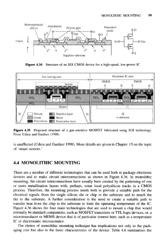
Figure 4.34 Structure of an SOI CMOS device for a high-speed, low-power IC
Figure 4.35 Proposed structure of a gas-sensitive MOSFET fabricated using SOI technology.
From Udrea and Gardner (1998)
is unaffected (Udrea and Gardner 1998). More details are given in Chapter 15 on the topic
of 'smart sensors.'
4.4 MONOLITHIC MOUNTING
There are a number of different technologies that can be used both to package electronic
devices and to make circuit interconnections as shown in Figure 4.36. In monolithic
mounting, the circuit interconnections have usually been created by the patterning of one
or more metallisation layers with, perhaps, some local polysilicon tracks in a CMOS
process. Therefore, the mounting process needs both to provide a suitable path for the
electrical signals from the single silicon die or chip to the substrate and to attach the
die to the substrate. A further consideration is the need to create a suitable path to
transfer heat from the chip to the substrate to limit the operating temperature of the 1C.
Figure 4.36 shows the four main technologies that are used to mount a chip that would
normally be standard components, such as MOSFET transistors or TTL logic devices, or, a
microtransducer or MEMS device that is of particular interest here, such as a temperature
IC or electrostatic microactuator.
The choice of monolithic mounting technique has implications not only to the pack-
aging cost but also to the basic characteristics of the device. Table 4.6 summarises the