
Page 119 - Microsensors, MEMS and Smart Devices - Gardner Varadhan and Awadelkarim
P. 119
100 STANDARD MICROELECTRONIC TECHNOLOGIES
Die-attach and wire-bond
Monolithic mounting Tape-automated bonding (TAB)
Flip-TAB mounting
Mounting
Flip-chip —I
Solder bump
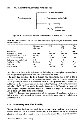
Figure 4.36 The different methods used to mount a monolithic die to a substrate
Table 4.6 Basic features of the four main monolithic mounting technologies. Adapted from Doane
and Franzon (1993)
Die attach and TAB Flip Flip
wire bond TAB Chip
Relative cost 1 >2 >2 0.8
Maximum I/O count 300-500 500-700 500-700 1000
Footprint size, die + (mm) 20-100 3-4 3-4 10
Lead inductance (nH) 2.0-3.5 4.0-5.0 4.0-5.0 <1.0
Peripheral bond pitch (mm) 4-7 3-4 3-4 10
Availability of die Excellent Fair Fair Poor
Probe test DC AC AC AC
Reworkability Poor Poor/Fair Fair Poor
basic features of these technologies and the following sections explain each method in
turn. Harper (1997) provides an excellent overview of this field.
In monolithic mounting, the die is bonded onto the substrate that is part of the IC
package. The IC package is then connected up to other electronic circuit components,
normally through a printed or hybrid circuit board. IC packages come in a variety of sizes
13
and forms, but the two main types are the dual-in-line package (DIP) and surface-mount
technology (SMT). DIPs are popular for smaller input-output (I/O) counts, whereas SMT
permits higher component densities. Figure 4.37 shows an example of a low-cost plastic
DIP, a metal DIP, and a metal SMT package.
Table 4.7 illustrates the characteristics of the common IC packages in terms of
their size, electrical characteristics, thermal characteristics, usual gates, and relative cost
(Ginsberg 1992).
4.4.1 Die Bonding and Wire Bonding
Die and wire bonding have been used for more than 25 years and involve a two-stage
process. First, the die is attached mechanically to the substrate either by an organic
adhesive, such as a silver-loaded epoxy, or by a metal solder. This is a low-temperature
13
Sometimes abbreviated to DIL package