
Page 116 - Microsensors, MEMS and Smart Devices - Gardner Varadhan and Awadelkarim
P. 116
MONOLITHIC PROCESSING 97
p-channel n-channel
Enhanced Enhanced
o V,
GS (off) GS (th) v, GS (th) OS (off)
Gate-source voltage V GS
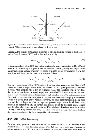
Figure 4.32 Variation of the channel conductance gds with gate-source voltage for the various
types of FETs when the drain-source voltage V DS is set to zero
Generally, the channel conductance is related to the drain-source voltage in the linear (1)
region from Equations (4.27) and (4.24), and is given by
/D
(4.33)
In the practical use of an FET, the various static and dynamic properties will be affected
when a load resistor R L is applied across the drain and source (see Figure 4.31) to create
a common-source voltage amplifier. However, when the output conductance is low, the
gain is related simply to the transconductance as follows:
(4.34)
The input capacitance of the FET transistor is an important parameter, and Figure 4.33
shows the principal capacitances within a transistor. A low-input capacitance is desirable
because, when coupled with a low on-resistance r ds(on), the switching time is very fast.
Short-channel transistors, such as those produced by the DMOS process, have very fast (i.e.
nanosecond) switching times and so are used in high-speed circuitry. The output capacitance
C ds is mainly determined by the n-p junction capacitance and is inversely proportional to the
square root of the drain-source voltage. However, the other capacitances depend on both
gate and drain voltages, threshold voltage, and parasitic capacitances. In all these cases,
it should be remembered that the device capacitances are in the picofarad range, so care
must be taken when designing and interfacing ICs and also while using transistors as either
sensing or actuating devices. Any stray capacitance will act as a charge divider and reduce
the voltage signals accordingly in a capacitive microtransducer.
4.3.5 SOI CMOS Processing
There are many processes now used for the fabrication of MOS ICs in addition to the
standard bulk processes described earlier. One that may have particular relevance to
microtransducers and MEMs is the SOI process. Notable successes have been made in