
Page 112 - Microsensors, MEMS and Smart Devices - Gardner Varadhan and Awadelkarim
P. 112
MONOLITHIC PROCESSING 93
n-type substrate
(a)
Y//////////////L Grow epitaxy Poly deposition and
gate mask
Grow SiO Etch oxide
Mask and etch Diffuse p body
n (arsenic)
Implant deep p+ implant
and oxidation
Deposit photoresist Grow oxide
mask and remove and mask
photoresist
Etch photoresist Source
Etch for source
contacts and
lay source
metal
Strip photoresist
Gate oxide
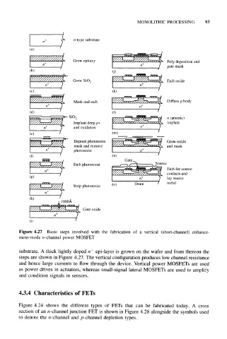
Figure 4.27 Basic steps involved with the fabrication of a vertical (short-channel) enhance-
ment-mode n -channel power MOSFET
substrate. A thick lightly doped n epi-layer is grown on the wafer and from thereon the
steps are shown in Figure 4.27. The vertical configuration produces low channel resistance
and hence large currents to flow through the device. Vertical power MOSFETs are used
as power drives in actuators, whereas small-signal lateral MOSFETs are used to amplify
and condition signals in sensors.
4.3.4 Characteristics of FETs
Figure 4.24 shows the different types of FETs that can be fabricated today. A cross
section of an n-channel junction FET is shown in Figure 4.28 alongside the symbols used
to denote the n-channel and p -channel depletion types.