
Page 110 - Microsensors, MEMS and Smart Devices - Gardner Varadhan and Awadelkarim
P. 110
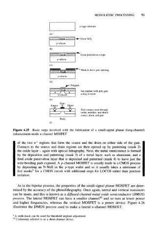
MONOLITHIC PROCESSING      91


                                        p-type substrate

                       (a)
                                        -Grow  SiO,
                           p-silicon
                       (b)
                                        Grow polysilicon n-type
                           p-silicon


                                         Mask to leave gate opening
                            p-silicon
                       (d)
                                   Polygate
                                         Ion-implant with poly gate
                                         acting as mask
                            p-silicon
                             Gate
                        Source  9  Drain
                                         Etch contact areas through
                                         oxide, metalize, and attach
                                         source, drain, and gate
                             Body
                       (0

   Figure  4.25  Basic  steps  involved  with  the  fabrication  of  a  small-signal  planar  (long-channel)
  enhancement-mode n-channel MOSFET

     of  the  two  n +  regions  that  form  the  source  and  the  drain  on  either  side  of  the  gate.
     Contacts  to  the  source  and  drain  regions  are  then  opened  up  by  patterning  (mask  2)
     the oxide  layer -  again  with optical  lithography.  Next, the metal  interconnect  is formed
     by  the  deposition  and  patterning  (mask  3)  of  a  metal  layer,  such  as  aluminum, and  a
     final  oxide  passivation  layer  that  is  deposited  and  patterned  (mask  4)  to  leave just  the
     wire-bonding  pads exposed.  A p-channel  MOSFET  is usually made in a CMOS  process
     by  depositing  an  N-Well  in  the  p-type  wafer  and  so  it  usually  takes  a  minimum of
     five  masks 9  for  a  CMOS  circuit with additional  steps  for  LOCOS  rather  than junction
     isolation.

     As in the bipolar  process, the properties of the small-signal planar MOSFET are deter-
  mined  by the accuracy  of the photolithography.  Once  again,  lateral and vertical  transistors
  can be made, and  this  is known  as a diffused-channel  metal  oxide  semiconductor  (DMOS)
  process. The  lateral  MOSFET  can  have  a  smaller  channel 10  and  so runs  at  lower  power
  and  higher  frequencies,  whereas  the  vertical  MOSFET  is  a  power  device.  Figure 4.26
  illustrates  the  DMOS  process  used  to  make  a  lateral  n-channel  MOSFET.

  9
    A sixth  mask can be used  for threshold implant  adjustment.
   10
     Commonly  referred  to as a short-channel  device.