
Page 108 - Microsensors, MEMS and Smart Devices - Gardner Varadhan and Awadelkarim
P. 108
MONOLITHIC PROCESSING 89
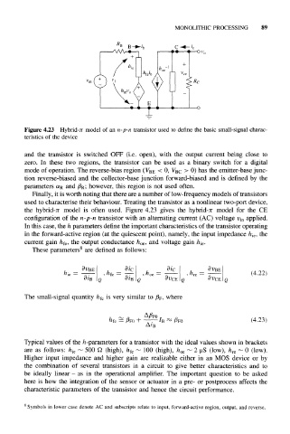
Figure 4.23 Hybrid- model of an n-p-n transistor used to define the basic small-signal charac-
teristics of the device
and the transistor is switched OFF (i.e. open), with the output current being close to
zero. In these two regions, the transistor can be used as a binary switch for a digital
mode of operation. The reverse-bias region (V BE < 0, V BC > 0) has the emitter-base junc-
tion reverse-biased and the collector-base junction forward-biased and is defined by the
parameters a R and B R; however, this region is not used often.
Finally, it is worth noting that there are a number of low-frequency models of transistors
used to characterise their behaviour. Treating the transistor as a nonlinear two-port device,
the hybrid- model is often used. Figure 4.23 gives the hybrid- model for the CE
configuration of the n-p-n transistor with an alternating current (AC) voltage v in applied.
In this case, the h parameters define the important characteristics of the transistor operating
in the forward-active region (at the quiescent point), namely, the input impedance h ie, the
current gain h fe, the output conductance h oe, and voltage gain h ie.
These parameters 8 are defined as follows:
BE , _ 'BE
5 "oe — h re= (4.22)
Q
The small-signal quantity h fe is very similar to B F, where
(4.23)
Typical values of the h -parameters for a transistor with the ideal values shown in brackets
are as follows: h ie ~ 500 (high), h fe ~ 100 (high), h oe ~ 2 uS (low), h re ~ 0 (low).
Higher input impedance and higher gain are realizable either in an MOS device or by
the combination of several transistors in a circuit to give better characteristics and to
be ideally linear - as in the operational amplifier. The important question to be asked
here is how the integration of the sensor or actuator in a pre- or postprocess affects the
characteristic parameters of the transistor and hence the circuit performance.
!
Symbols in lower case denote AC and subscripts relate to input, forward-active region, output, and reverse.