
Page 104 - Microsensors, MEMS and Smart Devices - Gardner Varadhan and Awadelkarim
P. 104
MONOLITHIC PROCESSING 85
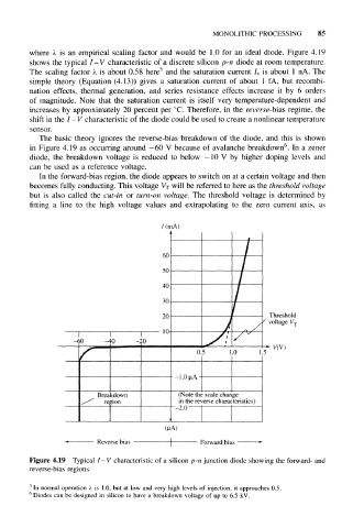
where is an empirical scaling factor and would be 1.0 for an ideal diode. Figure 4.19
shows the typical /- V characteristic of a discrete silicon p-n diode at room temperature.
The scaling factor A is about 0.58 here 5 and the saturation current I S is about 1 nA. The
simple theory (Equation (4.13)) gives a saturation current of about 1 fA, but recombi-
nation effects, thermal generation, and series resistance effects increase it by 6 orders
of magnitude. Note that the saturation current is itself very temperature-dependent and
increases by approximately 20 percent per °C. Therefore, in the reverse-bias regime, the
shift in the I - V characteristic of the diode could be used to create a nonlinear temperature
sensor.
The basic theory ignores the reverse-bias breakdown of the diode, and this is shown
6
in Figure 4.19 as occurring around —60 V because of avalanche breakdown . In a zener
diode, the breakdown voltage is reduced to below — 10 V by higher doping levels and
can be used as a reference voltage.
In the forward-bias region, the diode appears to switch on at a certain voltage and then
becomes fully conducting. This voltage V T will be referred to here as the threshold voltage
but is also called the cut-in or turn-on voltage. The threshold voltage is determined by
fitting a line to the high voltage values and extrapolating to the zero current axis, as
/(rnA)
Threshold
voltage V T
10
-60 -40 -20
V(V)
0.5 1.5
-l.0 uA
Breakdown (Note the scale change
region in the reverse characteristics)
--2.0
Reverse bias Forward bias
Figure 4.19 Typical I-V characteristic of a silicon p-n junction diode showing the forward- and
reverse-bias regions
5
In normal operation is 1.0, but at low and very high levels of injection, it approaches 0.5.
6
Diodes can be designed in silicon to have a breakdown voltage of up to 6.5 kV.