
Page 124 - Microsensors, MEMS and Smart Devices - Gardner Varadhan and Awadelkarim
P. 124
104 STANDARD MICROELECTRONIC TECHNOLOGIES
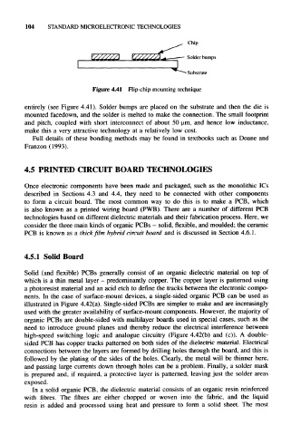
Chip
— Solder bumps
""-- Substrate
Figure 4.41 Flip-chip mounting technique
entirely (see Figure 4.41). Solder bumps are placed on the substrate and then the die is
mounted facedown, and the solder is melted to make the connection. The small footprint
and pitch, coupled with short interconnect of about 50 urn, and hence low inductance,
make this a very attractive technology at a relatively low cost.
Full details of these bonding methods may be found in textbooks such as Doane and
Franzon (1993).
4.5 PRINTED CIRCUIT BOARD TECHNOLOGIES
Once electronic components have been made and packaged, such as the monolithic ICs
described in Sections 4.3 and 4.4, they need to be connected with other components
to form a circuit board. The most common way to do this is to make a PCB, which
is also known as a printed wiring board (PWB). There are a number of different PCB
technologies based on different dielectric materials and their fabrication process. Here, we
consider the three main kinds of organic PCBs - solid, flexible, and moulded; the ceramic
PCB is known as a thick film hybrid circuit board and is discussed in Section 4.6.1.
4.5.1 Solid Board
Solid (and flexible) PCBs generally consist of an organic dielectric material on top of
which is a thin metal layer - predominantly copper. The copper layer is patterned using
a photoresist material and an acid etch to define the tracks between the electronic compo-
nents. In the case of surface-mount devices, a single-sided organic PCB can be used as
illustrated in Figure 4.42(a). Single-sided PCBs are simpler to make and are increasingly
used with the greater availability of surface-mount components. However, the majority of
organic PCBs are double-sided with multilayer boards used in special cases, such as the
need to introduce ground planes and thereby reduce the electrical interference between
high-speed switching logic and analogue circuitry (Figure 4.42(b) and (c)). A double-
sided PCB has copper tracks patterned on both sides of the dielectric material. Electrical
connections between the layers are formed by drilling holes through the board, and this is
followed by the plating of the sides of the holes. Clearly, the metal will be thinner here,
and passing large currents down through holes can be a problem. Finally, a solder mask
is prepared and, if required, a protective layer is patterned, leaving just the solder areas
exposed.
In a solid organic PCB, the dielectric material consists of an organic resin reinforced
with fibres. The fibres are either chopped or woven into the fabric, and the liquid
resin is added and processed using heat and pressure to form a solid sheet. The most