
Page 129 - Microsensors, MEMS and Smart Devices - Gardner Varadhan and Awadelkarim
P. 129
HYBRID AND MCM TECHNOLOGIES 109
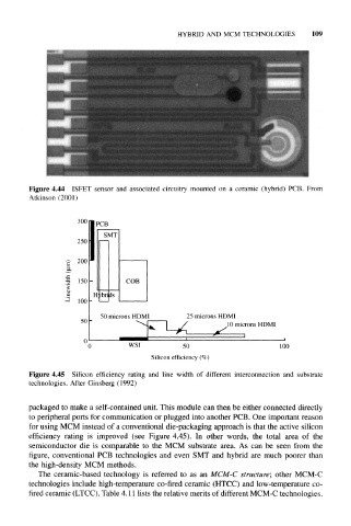
Figure 4.44 ISFET sensor and associated circuitry mounted on a ceramic (hybrid) PCB. From
Atkinson (2001)
PCB
SMT
250
200
brids
100
50 microns HDMI 25 microns HDMI
50
10 microns HDMI
0
0 WSI 50
Silicon efficiency (%)
Figure 4.45 Silicon efficiency rating and line width of different interconnection and substrate
technologies. After Ginsberg (1992)
packaged to make a self-contained unit. This module can then be either connected directly
to peripheral ports for communication or plugged into another PCB. One important reason
for using MCM instead of a conventional die-packaging approach is that the active silicon
efficiency rating is improved (see Figure 4.45). In other words, the total area of the
semiconductor die is comparable to the MCM substrate area. As can be seen from the
figure, conventional PCB technologies and even SMT and hybrid are much poorer than
the high-density MCM methods.
The ceramic-based technology is referred to as an MCM-C structure; other MCM-C
technologies include high-temperature co-fired ceramic (HTCC) and low-temperature co-
fired ceramic (LTCC). Table 4.11 lists the relative merits of different MCM-C technologies.