
Page 127 - Microsensors, MEMS and Smart Devices - Gardner Varadhan and Awadelkarim
P. 127
PRINTED CIRCUIT BOARD TECHNOLOGIES 107
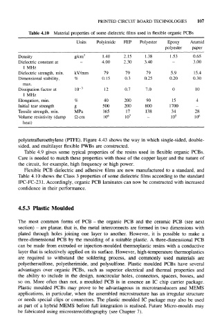
Table 4.10 Material properties of some dielectric films used in flexible organic PCBs
Units Polyimide FEP Polyester Epoxy Aramid
polyester paper
Density g/cm 3 1.40 2.15 1.38 1.53 0.65
Dielectric constant at 4.00 2.30 3.40 - 3.00
1 MHz
Dielectric strength, min. kV/mm 79 79 79 5.9 15.4
Dimensional stability, % 0.15 0.3 0.25 0.20 0.30
max.
Dissipation factor at 10 –3 12 0.7 7.0 0 10
1 MHz
Elongation, min. % 40 200 90 15 4
Initial tear strength g 500 200 800 1700 -
Tensile strength, min. MPa 165 17 138 34 28
Volume resistivity (damp Q-cm 10 6 10 7 - 10 5 10 6
heat)
polytetrafluroethylene (PTFE). Figure 4.43 shows the way in which single-sided, double-
sided, and multilayer flexible PWBs are constructed.
Table 4.9 gives some typical properties of the resins used in flexible organic PCBs.
Care is needed to match these properties with those of the copper layer and the nature of
the circuit, for example, high frequency or high power.
Flexible PCB dielectric and adhesive films are now manufactured to a standard, and
Table 4.10 shows the Class 3 properties of some dielectric films according to the standard
IPC-FC-231. Accordingly, organic PCB laminates can now be constructed with increased
confidence in their performance.
4.5.3 Plastic Moulded
The most common forms of PCB - the organic PCB and the ceramic PCB (see next
section) - are planar, that is, the metal interconnects are formed in two dimensions with
plated through holes joining one layer to another. However, it is possible to make a
three-dimensional PCB by the moulding of a suitable plastic. A three-dimensional PCB
can be made from extruded or injection-moulded thermoplastic resins with a conductive
layer that is selectively applied on its surface. However, high-temperature thermoplastics
are required to withstand the soldering process, and commonly used materials are
polyethersulfone, polyetherimide, and polysulfone. Plastic moulded PCBs have several
advantages over organic PCBs, such as superior electrical and thermal properties and
the ability to include in the design, noncircular holes, connectors, spacers, bosses, and
so on. More often than not, a moulded PCB is in essence an IC chip carrier package.
Plastic moulded PCBs may prove to be advantageous in microtransducers and MEMS
applications, in particular, when the assembled microstructure has an irregular structure
or needs special clips or connectors. The plastic moulded IC package may also be used
as part of a hybrid MEMS before full integration is realised. Future Micro-moulds may
be fabricated using microstereolithography (see Chapter 7).