
Page 131 - Microsensors, MEMS and Smart Devices - Gardner Varadhan and Awadelkarim
P. 131
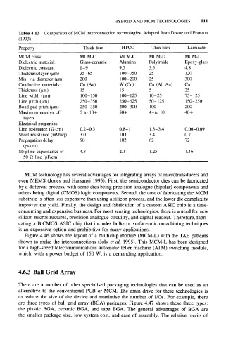
HYBRID AND MCM TECHNOLOGIES       111

  Table  4.13  Comparison  of MCM interconnection technologies. Adapted  from  Doane and Franzon
  (1993)

  Property                  Thick film     HTCC       Thin film     Laminate
  MCM   class             MCM-C           MCM-C      MCM-D         MCM-L
  Dielectric material:    Glass-ceramic   Alumina    Polyimide     Epoxy-glass
  Dielectric  constant    6-9             9.5        3.5           4.8
  Thickness/layer  (um)   35-65           100-750    25             120
  Min.  via diameter (urn)  200           100-200    25            300
  Conductive  materials:  Cu (Au)         W(Co)      Cu (Al, Au)   Cu
  Thickness (am)           15             15         5             25
  Line  width (um)         100-150        100-125     10-25        75-125
  Line  pitch (um)        250-350         250-625    50-125         150-250
  Bond  pad  pitch (um)   250-350         200-300     100          200
  Maximum number of       5  to  10+      50+        4-to 10       40+
    layers
  Electrical  properties:
  Line resistance  (£2 -cm)  0.2-0.3      0.8-1       1.3-3.4      0.06-0.09
  Sheet  resistance  (mfi/sq)  3.0        10.0       3.4           0.7
  Propagation  delay      90              102        62            72
    (ps/cm)
  Stripline  capacitance  of  4.3         2.1         1.25          1.46
    50  Q line  (pF/cm)


     MCM technology has several advantages for integrating arrays of microtransducers  and
  even  MEMS  (Jones  and  Harsanyi  1995).  First,  the  semiconductor  dies  can  be  fabricated
  by a different  process,  with some  dies being precision  analogue (bipolar) components and
  others  being digital  (CMOS) logic  components.  Second,  the cost of fabricating the MCM
  substrate is often  less expensive than using a silicon process,  and the lower die complexity
  improves  the  yield. Finally, the  design  and fabrication of  a custom ASIC  chip  is  a  time-
  consuming and expensive business. For most sensing technologies, there is a need for new
  silicon  microstructures, precision  analogue circuitry, and digital readout. Therefore, fabri-
  cating  a  BiCMOS  ASIC  chip  that  includes bulk-  or  surface-micromachining techniques
  is  an expensive  option  and  prohibitive  for many  applications.
     Figure 4.46 shows the layout of a multichip  module  (MCM-L)  with  the  TAB patterns
  shown  to  make  the  interconnections  (Joly  et al.  1995).  This  MCM-L  has  been  designed
  for  a high-speed  telecommunications  automatic teller  machine  (ATM) switching module,
  which,  with a  power  budget  of  150 W,  is a demanding  application.


  4.6.3  Ball  Grid  Array


  There  are  a  number  of  other  specialised  packaging  technologies  that  can  be  used  as  an
  alternative  to  the  conventional PCB  or  MCM.  The  main  drive  for  these  technologies  is
  to  reduce  the  size  of  the  device  and  maximise  the  number  of  I/Os. For  example,  there
  are  three  types of  ball  grid  array  (BGA) packages.  Figure 4.47 shows  these  three  types:
  the  plastic  BGA, ceramic  BGA, and  tape  BGA. The  general  advantages  of  BGA  are
  the  smaller package  size,  low  system  cost,  and  ease  of  assembly. The  relative  merits of