
Page 135 - Microsensors, MEMS and Smart Devices - Gardner Varadhan and Awadelkarim
P. 135
PROGRAMMABLE DEVICES AND ASICs 115
between devices according to where they were programmed. In this case, devices may
all be regarded as 'electrically' programmed and then they can be subdivided into those
programmed by the manufacturer (as in mask-programmed parts) and those programmed
by the user (as in field-programmable gate array).
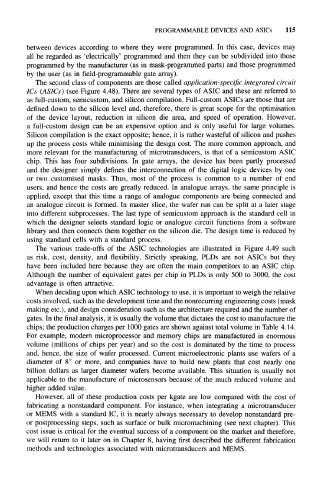
The second class of components are those called application-specific integrated circuit
ICs (ASICs) (see Figure 4.48). There are several types of ASIC and these are referred to
as full-custom, semicustom, and silicon compilation. Full-custom ASICs are those that are
defined down to the silicon level and, therefore, there is great scope for the optimisation
of the device layout, reduction in silicon die area, and speed of operation. However,
a full-custom design can be an expensive option and is only useful for large volumes.
Silicon compilation is the exact opposite; hence, it is rather wasteful of silicon and pushes
up the process costs while minimising the design cost. The more common approach, and
more relevant for the manufacturing of microtransducers, is that of a semicustom ASIC
chip. This has four subdivisions. In gate arrays, the device has been partly processed
and the designer simply defines the interconnection of the digital logic devices by one
or two customised masks. Thus, most of the process is common to a number of end
users, and hence the costs are greatly reduced. In analogue arrays, the same principle is
applied, except that this time a range of analogue components are being connected and
an analogue circuit is formed. In master slice, the wafer run can be split at a later stage
into different subprocesses. The last type of semicustom approach is the standard cell in
which the designer selects standard logic or analogue circuit functions from a software
library and then connects them together on the silicon die. The design time is reduced by
using standard cells with a standard process.
The various trade-offs of the ASIC technologies are illustrated in Figure 4.49 such
as risk, cost, density, and flexibility. Strictly speaking, PLDs are not ASICs but they
have been included here because they are often the main competitors to an ASIC chip.
Although the number of equivalent gates per chip in PLDs is only 500 to 3000, the cost
advantage is often attractive.
When deciding upon which ASIC technology to use, it is important to weigh the relative
costs involved, such as the development time and the nonrecurring engineering costs (mask
making etc.), and design consideration such as the architecture required and the number of
gates. In the final analysis, it is usually the volume that dictates the cost to manufacture the
chips; the production charges per 1000 gates are shown against total volume in Table 4.14.
For example, modern microprocessor and memory chips are manufactured in enormous
volume (millions of chips per year) and so the cost is dominated by the time to process
and, hence, the size of wafer processed. Current microelectronic plants use wafers of a
diameter of 8" or more, and companies have to build new plants that cost nearly one
billion dollars as larger diameter wafers become available. This situation is usually not
applicable to the manufacture of microsensors because of the much reduced volume and
higher added value.
However, all of these production costs per kgate are low compared with the cost of
fabricating a nonstandard component. For instance, when integrating a microtransducer
or MEMS with a standard IC, it is nearly always necessary to develop nonstandard pre-
or postprocessing steps, such as surface or bulk micromachining (see next chapter). This
cost issue is critical for the eventual success of a component on the market and therefore,
we will return to it later on in Chapter 8, having first described the different fabrication
methods and technologies associated with microtransducers and MEMS.