
Page 140 - Microsensors, MEMS and Smart Devices - Gardner Varadhan and Awadelkarim
P. 140
120 SILICON MICROMACHINING: BULK
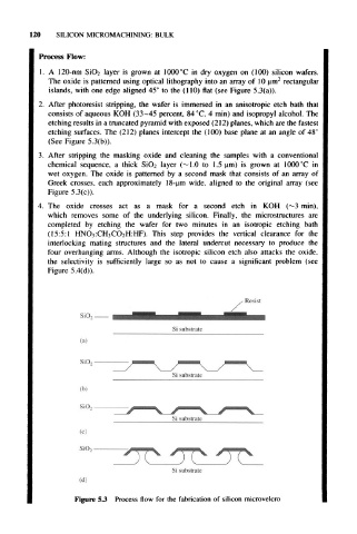
Process Flow:
1. A 120-nm SiO 2 layer is grown at 1000°C in dry oxygen on (100) silicon wafers.
The oxide is patterned using optical lithography into an array of 10 um 2 rectangular
islands, with one edge aligned 45° to the (110) flat (see Figure 5.3(a)).
2. After photoresist stripping, the wafer is immersed in an anisotropic etch bath that
consists of aqueous KOH (33-45 percent, 84 °C, 4 min) and isopropyl alcohol. The
etching results in a truncated pyramid with exposed (212) planes, which are the fastest
etching surfaces. The (212) planes intercept the (100) base plane at an angle of 48°
(See Figure 5.3(b)).
3. After stripping the masking oxide and cleaning the samples with a conventional
chemical sequence, a thick SiO 2 layer (~1.0 to 1.5 um) is grown at 1000 °C in
wet oxygen. The oxide is patterned by a second mask that consists of an array of
Greek crosses, each approximately 18-um wide, aligned to the original array (see
Figure 5.3(c)).
4. The oxide crosses act as a mask for a second etch in KOH (~3 min),
which removes some of the underlying silicon. Finally, the microstructures are
completed by etching the wafer for two minutes in an isotropic etching bath
(15:5:1 HNO 3:CH 3CO 2H:HF). This step provides the vertical clearance for the
interlocking mating structures and the lateral undercut necessary to produce the
four overhanging arms. Although the isotropic silicon etch also attacks the oxide,
the selectivity is sufficiently large so as not to cause a significant problem (see
Figure 5.4(d)).
Resist
SiO 2
Si substrate
(a)
SiO 2
Si substrate
(b)
Si0
Si substrate
Si substrate
(d)
Figure 5.3 Process flow for the fabrication of silicon microvelcro