
Page 144 - Microsensors, MEMS and Smart Devices - Gardner Varadhan and Awadelkarim
P. 144
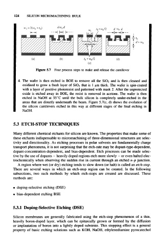
124    SILICON MICROMACHINING:  BULK

                           dw bd
                                           w,   'b+V2    d  w b d
            H—M          •H H  K-         K--H  /     ---Hh*-HK--


             (a)                                          (d)


               Figure 5.7  Four process  steps to make  and release the cantilever


     4.  The  wafer  is  then  etched  in  BOE  to  remove  all  the  SiO 2  and  is  then  cleaned  and
        oxidised  to  grow  a  fresh  layer  of  SiO 2  that  is  1 urn thick. The  wafer  is  spin-coated
        with a layer of positive photoresist and patterned with  mask 2. After  the unprotected
        oxide  is  etched  away  in  BOE,  the  resist  is  removed  in  acetone.  The  wafer  is  then
        etched  in  NaOH  at  55 °C  until  the  bulk  silicon  is  completely  under-etched  in  the
        areas that  are directly  underneath  the beam. Figure  5.7(c,  d)  shows  the  evolution of
        the  silicon  cantilevers  etched  in  this  way  at  different  stages  of  the  final  etching  in
        NaOH.


   5.3  ETCH-STOP     TECHNIQUES

   Many different  chemical etchants for silicon are known. The properties  that make some of
   these  etchants indispensable  to micromachining of three-dimensional  structures are  selec-
   tivity  and directionality.  As etching  processes  in polar  solvents  are  fundamentally  charge
   transport  phenomena, it is not surprising that the etch-rate  may be  dopant-type-dependent,
   dopant-concentration-dependent,  and bias-dependent.  Etch  processes  can  be  made  selec-
   tive by the use of dopants -  heavily doped regions etch more slowly -  or even halted elec-
   trochemically  when observing the  sudden rise in current through an etched  n-p junction.
     A region where wet (or dry) etching tends to slow down (or halt) is called  an etch-stop.
   There  are  several  ways  in  which  an  etch-stop  region  can  be  created.  In  the  following
   subsections,  two  such  methods  by  which  etch-stops  are  created  are  discussed.  These
   methods  are:

   •  doping-selective  etching  (DSE)

   •  bias-dependent etching BSE


   5.3.1  Doping-Selective  Etching  (DSE)

   Silicon  membranes  are  generally  fabricated  using  the  etch-stop  phenomenon  of  a  thin,
   heavily  boron-doped  layer,  which  can  be  epitaxially  grown  or  formed  by  the  diffusion
   or  implantation  of  boron  into a  lightly  doped  substrate.  This  stopping  effect  is a  general
  property  of  basic  etching  solutions  such  as  KOH,  NaOH,  ethylenediamine  pyrocatechol