
Page 148 - Microsensors, MEMS and Smart Devices - Gardner Varadhan and Awadelkarim
P. 148
128 SILICON MICROMACHINING: BULK
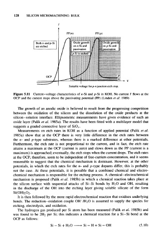
PP(n) PP(p)
::::•:•:• •:• !&*( •^ - - -— -=
j Oxide gr<)Wth | :!:|R:j: ^ Oxide growth
on n Si a - Mi S] on p-Si and
pass vat c)n /!!!!! IE passivation
[ p-S'i s etched m m m^-4-. -__-__-_
^fllrSSvt
I**,: , , ,| , i f_ - .^.-C. _=CH— S fi
^^\
Suitable voltage for p-n junction etch stop.
Figure 5.11 Current-voltage characteristics of n-Si and p-Si in KOH. No current / flows at the
OCP and the current stops above the passivating potential (PP) (Linden et al. 1989)
The growth of an anodic oxide is believed to result from the progressing competition
between the oxidation of the silicon and the dissolution of the oxide products at the
silicon-solution interface. Ellipsometric measurements have given evidence of such an
oxide layer (Palik et al. 1985a). The results have been fitted with a multilayer model that
suggests a graded connective layer of SiO x.
Measurements on etch rates in KOH as a function of applied potential (Palik et al.
1985a) show that at the OCP there is very little difference in the etch rates between
the n- and p-type substrates, whereas there is a marked difference at other potentials.
Furthermore, the etch rate is not proportional to the current, and in fact, the etch rate
attains a maximum at the OCP (current is zero) and slows down as the PP (current is a
maximum) is approached; eventually, the etch stops when the current drops. The etch rates
at the OCP, therefore, seem to be independent of free-carriers concentration, and it seems
reasonable to suggest that the chemical mechanism is dominant. However, at the other
potentials, in which the etch rates for the n- and p-type dopants differ, this is probably
not the case. At these potentials, it is possible that a combined chemical and electro-
chemical mechanism is responsible for the etching process. A chemical-electrochemical
mechanism is proposed (Palik et al. 1985b) in which a chemical reaction takes place at
the silicon surface with sequential attacks of Si-Si bonds by H 2O and OH, resulting
in the discharge of the OH into the etching layer giving soluble silicate of the form
Si(OH) 2O 2.
It is then followed by the more rapid electrochemical reaction that oxidises underlying
–
bonds. The reduction-oxidation couple OH /H 2 O is assumed to supply the species for
etching, electrolysis, and oxidation.
The hydrogen gas produced per Si atom has been measured (Palik et al. 1985b) and
was found to be 2H 2 per Si; this indicates a chemical reaction for a Si—Si bond at the
OCP as follows:
Si - Si + H 2O Si - H + Si - OH (5.10)