
Page 149 - Microsensors, MEMS and Smart Devices - Gardner Varadhan and Awadelkarim
P. 149
ETCH-STOP TECHNIQUES 129
and
–
Si - Si + Si - OH + OH Si - O + Si - OH + H 2 (5.11)
The net reaction for dissolution of a silicon atom would, therefore, be
–
Si + 2HO + 2OH – > H 2 + Si(OH) 2 (O ) 2 (5.12)
The nature of the band bending at the surface will play a critical role in the effect that an
+
applied bias gives. A model relating the DSE and the p -Si etch-stop with band bending
and charge transfers has been suggested but is beyond the scope of this book.
The conventional electrochemical etch-stop technique is an attractive method for fabri-
cating both microsensors and microactuators because it has the potential for allowing
reproducible fabrication of moderately doped n-type silicon microstructures with good
thickness control. However, a major limiting factor in the use of the conventional elec-
trochemical etch-stop process is the effect of reverse-bias leakage current in the junction.
Because the selectivity between n- and p-type silicon in this process is achieved through
the current-blocking action of the diode, any leakage in this diode will affect the selec-
tivity. In particular, if the leakage current is very large, it is possible for etching to
terminate well before the junction is reached. In some situations, the etching process
may fail completely because of this leakage. This effect is well known, and alternative
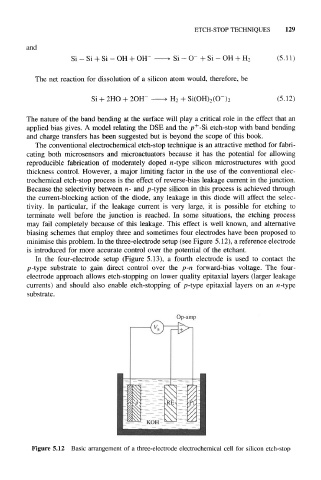
biasing schemes that employ three and sometimes four electrodes have been proposed to
minimise this problem. In the three-electrode setup (see Figure 5.12), a reference electrode
is introduced for more accurate control over the potential of the etchant.
In the four-electrode setup (Figure 5.13), a fourth electrode is used to contact the
p-type substrate to gain direct control over the p-n forward-bias voltage. The four-
electrode approach allows etch-stopping on lower quality epitaxial layers (larger leakage
currents) and should also enable etch-stopping of p-type epitaxial layers on an n-type
substrate.
Figure 5.12 Basic arrangement of a three-electrode electrochemical cell for silicon etch-stop