
Page 154 - Microsensors, MEMS and Smart Devices - Gardner Varadhan and Awadelkarim
P. 154
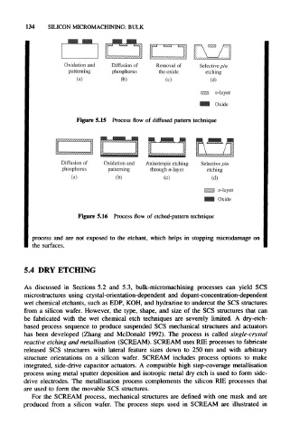
134    SILICON MICROMACHINING:  BULK


                  Oxidation and  Diffusion  of  Removal of  Selective p/n
                   patterning    phosphorus    the oxide     etching
                      (a)          (b)           (c)          (d)

                                                           tzza  n-layer
                                                           •I   Oxide

                     Figure  5.15  Process flow of diffused  pattern  technique


                                            m  jjjjjj^  m
                \


                 Diffusion  of  Oxidation and  Anisotropic etchin  Selective p/n
                  phosphorus    patterning  through n-layer   etching
                    (a)           (b)            (c)           (d)

                                                             V777A  n-layer
                                                             ^H  Oxide

                      Figure 5.16  Process flow of etched-pattern  technique


        process  and  are  not  exposed  to  the  etchant,  which  helps  in  stopping  microdamage on
        the  surfaces.


     5.4  DRY   ETCHING

     As  discussed  in  Sections  5.2  and  5.3,  bulk-micromachining  processes  can  yield  SCS
     microstructures  using  crystal-orientation-dependent  and  dopant-concentration-dependent
     wet chemical  etchants,  such as EDP,  KOH, and hydrazine  to undercut the SCS structures
     from  a  silicon  wafer. However,  the  type,  shape,  and  size  of  the  SCS  structures that can
     be  fabricated  with  the  wet  chemical  etch  techniques  are  severely  limited.  A  dry-etch-
     based  process  sequence  to  produce  suspended  SCS  mechanical  structures  and  actuators
     has  been  developed  (Zhang  and  McDonald  1992).  The  process  is  called single-crystal
     reactive etching and metallisation (SCREAM). SCREAM uses RIE processes  to fabricate
     released  SCS  structures  with  lateral  feature  sizes  down  to  250  nm  and  with  arbitrary
     structure  orientations  on  a  silicon  wafer.  SCREAM  includes  process  options  to  make
     integrated,  side-drive  capacitor  actuators.  A compatible  high  step-coverage  metallisation
     process  using metal  sputter deposition  and  isotropic  metal dry etch  is  used  to  form  side-
     drive  electrodes.  The  metallisation  process  complements  the  silicon  RIE  processes  that
     are  used  to  form the  movable  SCS  structures.
        For  the  SCREAM  process,  mechanical  structures  are  defined  with one  mask  and  are
     produced  from  a  silicon  wafer.  The  process  steps  used  in  SCREAM  are  illustrated in