
Page 155 - Microsensors, MEMS and Smart Devices - Gardner Varadhan and Awadelkarim
P. 155
Photoresist
Thermal SiO 2
Thermal SiO 2
Si substrate Si substrate
(b)
•••§ Thermal SiO 2 Thermal SiO 2
~U1_T
Si sulostrate
Si substrate
(c) (d)
Photoresist
— Aluminum
Aluminum
Thermal SiO 2
Thermal SiO 2 Si substrate
Si substrate
(0
Photoresist Aluminum
Aluminum
Silicon
Thermal SiO 2
Thermal SiO 2
Si substrate
Si substrate
(g) (h)
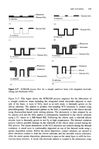
Figure 5.17 SCREAM process flow for a straight cantilever beam with integrated electrodes
(Zhang and McDonald 1992)
Figure 5.17. This figure shows the SCREAM process sequence for the fabrication of
a straight cantilever beam including the integrated metal electrodes adjacent to each
side of the beam. A layer of SiO 2, used as an etch mask, is thermally grown on the
silicon substrate. The pattern to produce free-standing SCS structures is created using
photolithography. The photoresist pattern on the SiO 2 is transferred to the silicon dioxide
using fluorocarbon-based oxide etching plasma. The photoresist is then stripped by an
O2 plasma etch and the SiO 2 pattern is subsequently transferred to the silicon substrate
using a Cl – -based or a HBr-based RIE. Following the silicon etch, a sidewall silicon
dioxide layer is thermally grown in wet O 2 at high temperatures. The thermal oxidation
process reduces possible damage on the sidewalls of the silicon steps created during the
RIE process. The lateral dimensions of the SCS structures are reduced during the thermal
oxidation. A metal layer is conformably deposited on top of the thermal oxide using a
sputter deposition system. Before the metal deposition, contact windows are opened to
allow electrical contact to both the silicon substrate and the movable silicon structures.
After the metal sputter deposition, photoresist is spun on the metal layer to refill the few-
microns-deep trenches. A metal side-electrode pattern is created in the photoresist using